
Professional PCB manufacturing and assembly
Building 6, Zone 3, Yuekang Road,Bao'an District, Shenzhen, China
+86-13410863085Mon.-Sat.08:00-20:00

The professional 32 layer PCB rapid proofing is used in the circuit board. If there is signal transmission, it is hoped that the signal can be transmitted from the sending end of the power supply to the receiving end smoothly with the minimum energy loss, and the receiving end will fully absorb it without any reflection. To achieve this kind of transmission, the impedance in the line must be equal to the impedance inside the transmitter to be called "impedance matching". When designing high-speed PCB circuits, impedance matching is one of the elements of design. The impedance value is absolutely related to the wiring mode. For example, whether to walk on the surface layer (Microstrip) or the inner layer (Stripline/Double Stripline), the distance from the reference power layer or layer, the routing width, PCB material, etc. will affect the characteristic impedance value of the routing. In other words, the impedance value can only be determined after wiring, and the characteristic impedance produced by different PCB manufacturers also has slight differences. General simulation software can't take into account some discontinuous impedance wiring due to the limitation of the line model or the mathematical algorithm used. At this time, only some terminators, such as series resistors, can be reserved on the schematic diagram to mitigate the effect of discontinuous impedance wiring. The real fundamental solution to the problem is to avoid impedance discontinuity when wiring.
Process Flow and Technology of Multilayer Board
Core board production - laminated RCC - laser drilling - hole electroplating - pattern transfer - etching and film stripping - laminated RCC - integrated printed circuit board (HDI/BUM board) that is repeatedly formed into an anb structure.
(Note 1): The core plates here refer to various kinds of plates, such as conventional double-sided, multilayer plates, buried/blind hole multilayer plates, etc. However, these core plates must be blocked and polished before they can be laminated.
(Note 2): The HDI/BUM multilayer board structure can be represented by the f
ollowing formula.
a n b
A - is the number of layers on one side, n - is the core board, and b - is the number of layers on the other side.
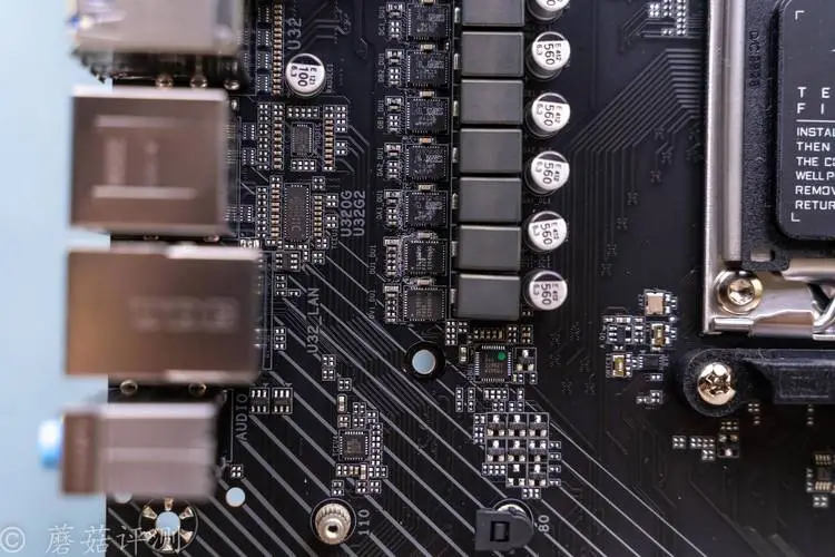
The guarantee of performance depends on PCB design, which everyone has realized. The performance test results of the same logic connection, the same device and different PCBs are different. Good design not only has high stability, but also can pass various demanding tests. But it is impossible to achieve this effect if the design is not ideal. In some low-end products, many manufacturers use the same chipsets and similar logical connections. The only difference is the level of PCB design. The difference of products is mainly reflected in PCB design. Fast proofing of 32 layer circuit board
The ease of processing is also an important indicator of PCB design. Good PCB design is convenient for processing, maintenance, testing and manufacturing. The quality of PCB is not only related to the production efficiency of PCB manufacturers and SMT manufacturers, but also to the convenience of our testing and debugging.
PCB proofing
The difference between hardware and software of PCB board
It is divided into rigid circuit board and flexible circuit board.
The visual difference between rigid PCB and flexible PCB is that flexible PCB can be bent. The common thickness of rigid PCB board is 0.2mm, 0.4mm, 0.6mm, 0.8mm, 1.0mm, 1.2mm, 1.6mm, 2.0mm, etc. The common thickness of flexible PCB is 0.2mm. Thickening layer will be added at the back of the part to be welded. The thickness of the thickening layer varies from 0.2mm to 0.4mm. The purpose of understanding these is to provide structural engineers with a spatial reference when designing. Common materials of rigid PCB board include phenolic paper laminate, epoxy paper laminate, polyester glass felt laminate, and epoxy glass cloth laminate; Common materials of flexible PCB board include: polyester film, polyimide film, fluorinated ethylene propylene film.
Process requirements for fast PCB welding of 32 layer circuit board
2.1 Process requirements for component processing
2.1.1 Before the components are inserted, the solderability of the components must be treated. If the solderability is poor, the components' pins must be tinned first.
2.1.2 After the pins of components are shaped, the pin spacing shall be consistent with the bonding pad hole spacing corresponding to the PCB board.
2.1.3 The shape of component pin processing shall be conducive to heat dissipation during component welding and mechanical strength after welding.
2.2 Process requirements for component insertion on PCB
2.2.1 The insertion sequence of components on PCB board is from low to high, from small to large, from light to heavy, from easy to difficult, from general components to special components, and the installation of the previous process shall not affect the installation of the next process.
2.2.2 After the components are inserted, their marks shall be read from left to right as far as possible in a direction that is easy to read.
2.2.3 Polarity of components with polarity shall be installed in strict accordance with the requirements of the drawings, and wrong installation is not allowed.
2.2.4 The insertion of components on PCB board shall be evenly distributed, neatly arranged and beautiful, and oblique arrangement, vertical crossing and overlapping arrangement are not allowed; One side is not allowed to be high while the other side is low; It is also not allowed that one side of the pin is long and the other side is short.
2.3 Process requirements for PCB solder joints
2.3.1 The mechanical strength of welding points shall be sufficient
2.3.2 Reliable welding to ensure conductivity
2.3.3 The surface of welding points shall be smooth and clean
The demand for 94HB single-sided cardboard proofing is not very large, so it is impossible to put a large number of 94HB single-sided cardboard panels together for proofing, but to use a single sheet for production. Therefore, the cost is generally 200. Many people are also surprised that 94HB single-sided cardboard is a paper substrate, which is a relatively cheap product, and FR-4 fiberglass board is a mid end product. This is why the price of proofing is still expensive.


Just upload Gerber files, BOM files and design files, and the KINGFORD team will provide a complete quotation within 24h.