
Professional PCB manufacturing and assembly
Building 6, Zone 3, Yuekang Road,Bao'an District, Shenzhen, China
+86-13410863085Mon.-Sat.08:00-20:00


Reliability Design Scheme of Mobile Phone PCB
Because of the uncertainty in theory, RF PCB design is usually described as "black art", but this view is only partially correct RF board design has many rules that can be followed and should not be ignored However, in practical design, the really useful technology is how to compromise these principles and laws when they cannot be accurately implemented due to various design constraints Of course, there are many important RF design topics worth discussing, including impedance and impedance matching, insulation layer information and laminates, wavelength and standing wave. In addition, these have a great impact on the EMC and EMI of mobile phones
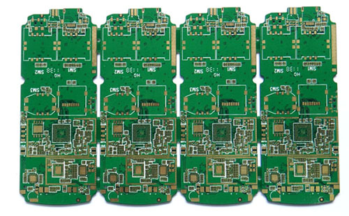
PCB board

1 Isolate high power RF amplifier (HPA) and low noise amplifier (LNA) as far as possible. In short, keep the high power RF transmitting circuit away from the low power RF receiving circuit Mobile phones have more functions and many components, but the space of PCB board is very small. Considering the design process of wiring limitation, all these require relatively high design skills At this point, you may need to design four to six PCB layers to work alternately instead of simultaneously High power circuits may also times include RF buffers and voltage controlled oscillators (VCO) Ensure that at least one full layer of high power area on the PCB is free of holes Of course, the more copper, the better Sensitive analog signals shall be as far away from high-speed digital signals and RF signals as possible
2. The design area can be divided into physical area and electric area Physical partition mainly involves component layout, orientation and mask, etc The power partition can be further divided into distribution partition, RF wiring, sensitive circuits and signals, and grounding
2.1 We discuss physical zoning Component layout is the key to RF design Effective technology is to first fix the components on the RF path and orient them, so as to reduce the length of the RF path to keep the input away from the output, and to separate high power and low power circuits as much as possible An efficient way to stack circuit boards is to place the main ground floor (the main ground) on the second layer below the surface Reducing the size of the through-hole in the RF path can not only reduce the path inductance, but also reduce the opportunities for virtual solder joints on the main ground and RF energy leakage to other areas in the laminate In physical space, linear circuits such as multistage amplifiers are usually enough to isolate multiple RF areas from each other, but duplexers, mixers, and IF amplifiers/mixers always have multiple RF/IF signals interfering with each other. Therefore, care must be taken to reduce this effect to
2.2 RF and IF should be crossed and separated as much as possible The correct RF path is very important to the performance of the entire PCB, which is why component layout usually takes up most of the time in mobile PCB design In the design of mobile phone PCB, it is usually possible to place the low noise amplifier circuit on one side of the PCB, place the high-power amplifier on the other side, and finally connect it to the RF and baseband processor antennas on the same side through the bucket Some skills are needed to ensure that the through hole does not transfer RF energy from one side of the circuit board to the other. A common technology is to use blind holes on both sides By arranging through holes in the areas without RF interference on both sides of the PCB, the adverse effects of through holes can be minimized Sometimes it is not possible to ensure adequate isolation between multiple circuit blocks. In this case, metal masks must be considered to mask the RF energy in the RF area The metal mask must be installed on the ground and kept at a reasonable distance from the components, thus occupying valuable PCB space It is important to ensure the integrity of the mask as much as possible The digital signal line entering the metal mask cover shall pass through the inner layer as far as possible, and the layer below the PCB wiring layer is the stratum The RF signal line can be led out from the small gap at the bottom of the metal mask cover and the wiring layer of the gap, but the surrounding gap should be laid on the ground as much as possible, and the grounding on different layers can be connected through multiple holes
2.3 Proper and effective chip power decoupling is also very important Many RF chips with integrated linear circuits are very sensitive to power supply noise. Generally, each chip needs up to four capacitors and an isolation inductor to ensure that all power supply noise is filtered Integrated circuits or amplifiers usually have open drain outputs. In retrospect, a pull-up inductor is required to provide high impedance RF loads and low impedance DC power The same principle also applies to the decoupling of power supply at the inductive end Some chips need more power to work, so you may need two or three groups of capacitors and inductors to decouple separately. Several inductors are connected in parallel, because this will form interference signals of tubular transformers and transformers. Therefore, the distance between them must be at least equal to the height of one of the devices, or at a right angle to the mutual inductance
2.4 The principle of power partition is usually the same as that of physical partition, but there are other factors Some parts of the phone work under different voltages and are controlled by software to extend battery life This means that the mobile phone needs to use multiple power supplies, which brings more problems to isolation The power supply is usually introduced from the connector, immediately decoupled to filter out any noise from outside the circuit board, and then distributed through a set of switches or regulators The DC current of most circuits on the mobile phone PCB is relatively small, so the wiring width is usually not a problem. However, it is necessary to run a separate large current line as wide as possible for the power supply of the high-power amplifier to reduce the transmission voltage to To avoid excessive current loss, multiple holes are used to transfer current from one layer to another In addition, if the power pin of the high power amplifier is not fully decoupled, the high power noise will radiate to the entire circuit board and cause various problems The grounding of high power amplifier is very important, and a metal mask is usually required In most cases, it is also important to ensure that the RF output is kept away from the RF input This also applies to amplifiers, buffers, and screening programs In a bad case, if the outputs of amplifiers and buffers respond to their inputs with the correct phase and amplitude, they can generate self-excited oscillations In this case, they will be able to operate stably at any temperature and voltage In fact, they may become unstable and add noise and intermodulation to the RF signal If the RF signal line must be wound from the input to the output of the filter, the band-pass characteristics of the filter will be seriously damaged In order to achieve good isolation between input and output, a field must be laid around the screening program first, and then a field must be placed in the lower area of the filter and connected to the main ground around the filter It is also a good idea to place the signal wire that needs to pass through the filter as far away from the filter pin as possible
2.5 To ensure no new noise, the following aspects must be considered: first, the expected bandwidth range of the control line can be DC to 2MHz, and it is almost impossible to remove such broadband noise through filtering; Second, the VCO control circuit is usually a part of the reverberation loop of the control frequency, which can introduce noise in many places. In addition, the VCO control circuit must be handled carefully Ensure that the RF floor is secure and that all components are securely connected to the main floor and isolated from other wires that may cause noise In addition, to ensure that the power supply of the VCO is fully decoupled, special attention must be paid to the VCO, because its RF output is often at a relatively high level, and the output signal of the VCO is easy to interfere with other circuits In fact, VCO is usually placed at the end of RF area, sometimes it needs a metal mask Resolvent circuits (one for the transmitter, the other for the receiver) are related to the VCO, but have their own characteristics In short, the resonant circuit is a parallel resonant circuit with a capacitor diode, which helps to set the operating frequency of the voltage controlled oscillator and modulate voice or data into RF signals All VCO design principles also apply to resonant circuits Resonant circuits are usually very sensitive to noise because they contain a large number of components, have a wide distribution area on the circuit board, and usually operate at high frequencies The signals are usually arranged on the adjacent pins of the chip, but these pins need to be paired with relatively large inductors and capacitors to work, which in turn requires that these inductors and capacitors be closely placed together and connected back to the noise sensitive control loop It is not easy to do this
3. Pay attention to the following aspects of PCB board in mobile phone design
3.1 Processing of power supply and ground cable
Even if the wiring in the overall PCB is well completed, but the interference caused by the power supply and ground wire is not well considered, and the product efficiency will decline, sometimes even affecting the success rate of the product Therefore, the electrical wiring and grounding wire should be carefully handled. The electrical noise interference will cause the drop limit at the grounding wire, so as to ensure the product quality For every engineer engaged in electronic product design, it is obvious that the reason for the noise between the ground wire and the power line is that Now, the reduced noise suppression is only described as follows:
(1) It is well known that the decoupling capacitor is added between the power supply and ground wire.
(2) As far as possible to width the width of power supply, the ground wire is: ground wire>power line>signal line. Generally, the signal line width is 0.2~0.3mm, the fine width can reach 0.05~0.07mm, and the power line is 1.2~2.5mm This PCB digital circuit can be composed of a ground network for use (analog circuit ground cannot be used in this way)
(3) With a large area of copper layer for ground Or it can be made into a multilayer board, power supply, and a layer of grounding wire
3.2 Common ground processing of digital circuit and analog circuit
Many PCBS are no longer single function circuits (digital or analog) Therefore, when wiring, we need to consider the interference between them, especially the noise interference on the ground wire Digital circuit has high frequency and analog circuit has strong sensitivity For signal lines, high-frequency signal lines should be as far away from sensitive analog circuit equipment as possible As for the ground wire, the whole PCB board has only one node to the outside world. Therefore, the digital and analog common grounding problem must be solved internally for the PCB board In the circuit board, digital grounding and analog grounding are actually independent of each other, only in the PCB board and the external connection interface (such as plug, etc.) There is a short circuit between digital ground and analog ground Note that there is only one connection point There are also some uncommon problems with PCB boards, depending on the system design
3.3 Signal Cables Are laid on electrical (ground) layers
In the multi layer PCB wiring, because there is no remaining finished product line in the signal line layer, additional layers will cause waste, and will also add a certain amount of workload and cost. To solve this conflict, you can consider wiring in the electrical (ground) layer The power area and the second formation should be considered first Because it keeps the integrity of the formation


Just upload Gerber files, BOM files and design files, and the KINGFORD team will provide a complete quotation within 24h.