
Professional PCB manufacturing and assembly
Building 6, Zone 3, Yuekang Road,Bao'an District, Shenzhen, China
+86-13410863085Mon.-Sat.08:00-20:00


Hardware Circuit Design of PCB Board Tester Based on FPGA
In order to improve the testing speed of PCB board tester, simplify the design of PCB, and improve the reconfiguration of the system and the convenience of test calculation transplantation, a hardware control system design scheme based on single-chip microcomputer PCB board proposes a FPGA based tester In the design, the field programmable gate array (FPGA) EP1K50 of Altera Corporation is selected, and the EDA design tool Synplify is used to complete the hardware design and debugging of the control system. Modelsim model, Quartz II, and Verilog hardware description language solve the problem that traditional circuits are difficult to implement The basic test principle of PCB light tester is Ohm's law The test method is to add a certain test voltage between the points to be tested, use the decoding circuit to select the PCB to be used, and obtain the corresponding resistance value between the two points The voltage signal is used to test the resistance or continuity between two points through the voltage comparison circuit Repeat the above steps several times to test the entire circuit board Because of a large number of test points, the general test machine exceeds 2048 points, and the test control circuit is more complex The search method and switching method of test points directly affect the test speed of the tester This paper studies the design of hardware control system based on FPGA
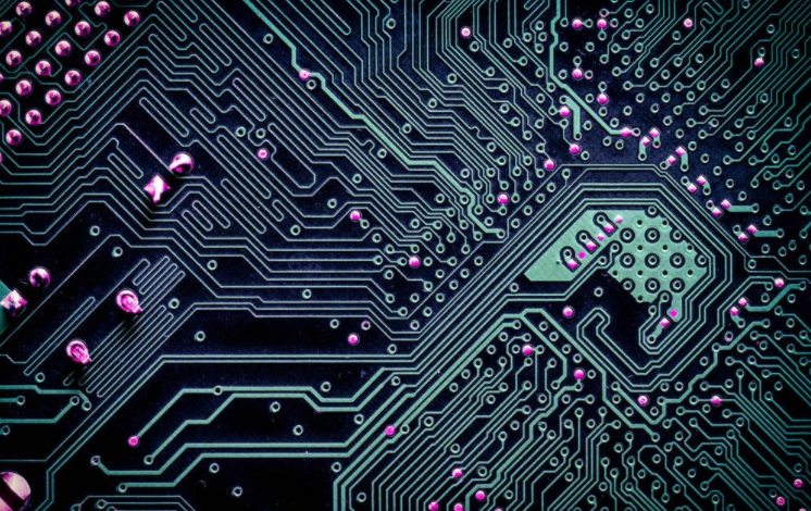
PCB board

Hardware control system
The test process is to control the test circuit to open different test switches under the control of the host. The test machine system consists of the following parts: PC 104, test control logic (implemented by FPGA) and high-voltage test circuit. The upper computer mainly completes human-computer interaction, test calculation, test data processing, control output and other functions. FPGA controls the high-voltage test circuit to complete the test process of PCB. The system uses PC104 as the upper computer and FPGA as the upper computer to control the test through PC104 bus.
Interface circuit between FPGA and PC104
PC104 busbar is an industrial control busbar specially defined for embedded control, and its signal definition is basically the same as ISA busbar. PC104 busbar has four busbar cycles, namely 8-bit busbar cycle, 16 bit busbar cycle, DMA busbar cycle and redraw busbar cycle. The 16 bit I/O bus cycle is 3 clock cycles, and the 8 bit I/O bus cycle is 6 clock cycles. In order to improve communication speed, ISA bus adopts 16 bit communication mode, namely 16 bit I/O mode. In order to make full use of the resources of PC104, FPGA is configured online after expanding the system bus bar of PC104. During normal operation, FPGA communicates with FPGA through PC104 bus bar.
Interface between FPGA and Serial A/D and D/A Devices
According to the system design requirements of the tester, it is necessary to conduct self-test on the test voltage and dual channel reference voltage, that is, at least 3 a/D conversion channels. The reference voltage of the two comparison circuits is output by D/A. The D/A channel of this system requires two channels. In order to reduce the number of control signal lines of A/D and D/A, tandem A/D and D/A devices are selected. Considering efficiency, price and other factors, the selected A/D equipment is TLC2543, and the selected D/A equipment is TLV5618. TLV5618 is a dual 12 bit voltage output DAC with buffered reference input (high impedance) from TI and digital control via CMOS compatible 3-wire serial bus. The device accepts a 16 bit command word and generates two D/a class ratio outputs. The TLV5618 has only one input/output cycle, which is determined by the external clock SCL K, lasts for 16 clock cycles, writes the command word to the on-chip register, and performs D/a conversion after completion. The TLV5618 read command word is valid from the falling edge of CS, and reads data from the falling edge of the next SCLK. After reading 16 bit data, it enters the conversion cycle until the next falling edge of CS appears. TLC2543 is a 12 bit switched capacitor successive approximation a/D converter with tandem control and 11 inputs from TI. The on-chip converter has the characteristics of high speed, high precision and low noise. The working process of TLC2543 is divided into two cycles: input/output cycle and conversion cycle. The input/output cycle is determined by the external clock SCLK, which lasts for 8, 12 or 16 clock cycles, and performs two operations at the same time: input 8-bit data to the on-chip register in MSB mode on the rising edge of SCLK; Output in MSB mode on the falling edge of SCLK 8, 12 and 16 bit conversion results. The conversion cycle starts from the falling edge of SCLK in the input/output cycle until the EOC signal becomes higher, indicating that the conversion is completed. In order to be consistent with the input/output cycle of TLV5618, MSB method is adopted and the 16 clock transmission timing of CS is used.
Since these two devices are SPI interfaces, they can be connected to the same SPI bus and run on different devices through different chip selection signals. Because the SPI interface protocol is very complex, as shown in Figure 3, the timing of these two devices does not use all SPI interface timing. In order to achieve the timing in line with the above logic and reduce the waste of FPGA resources in standard SPI interface IP check, the design adopts Verilog hardware description language to implement the design method of synchronous state machine (FSM), and compiles the C and DAC to control the timing. In fact, the program is a nested state machine. The main state machine and the bus started by the slave state machine through the control line form a finite state machine, which has different functions under different input signal conditions. It can be seen from Figure 3 that there are 4 states for analog digital conversion operation and 7 states for analog digital conversion operation. Several of the two states are the same, and the finite state machine can be used to complete the serial a/D and D/a operations. The program is actually a nested state machine. The main state machine and the bus started by the slave state machine through controlling the bus form a more complex finite state machine, which has different functions under different input signals. The drive clock (SCLK) and data bus (SI, SO) are operated by A/D and D/A. Since the write cycle of the operation has 16 clock cycles and the read cycle has 12 clock cycles, the module is completed in three nested finite state machines. In the system design, AD and DA operations are encapsulated into a single module, and the upper control module outputs command words and control signals to start the corresponding operations of the module. After the operation is completed (entering the idle state), the module sends the corresponding status signal to the upper module.
FPGA Programming Framework
FPGA on-chip program is the key to the correct operation of the entire test system. According to the top-down FPGA design principle, the system is divided into five independent modules, namely communication module (ISA), test module (test), AD/DA module, decoding module (decoder) and RAM control module (RAMCTL). ISA module: system communication and control module, which completes communication with the host, command word interpretation, control signal generation, etc. The system starts the ADDA module and completes the output of reference voltage according to the conduction resistance, insulation voltage and other parameters transmitted by the host; Start the test module and complete the test process according to the test command. Data is transmitted between multiple synchronous state machines running synchronously, which makes it more difficult to control data communication and data synchronization between multiple trips. RAM control module: before the test, the host transmits the test point information to the ISA module through the bus, and the ISA module stores it in the on-chip RAM; After the test is completed, the test results in RAM are transmitted to the host. During the test, the test module opens the corresponding test switch by reading the information of the test points in RAM, and then saves the test results in RAM. In this way, both modules need to read and write RAM to realize data sharing between the two modules. This requires a control signal to connect two groups of read and write signal lines to the RAM module, and the RAM control module completes this function. Test module: although there are various test programs, such as switch card self inspection, continuity test, insulation test, etc., the test program is the same, that is, test scanning. The test process is: add the reference voltage of the comparison circuit - open the switch of the point to be tested - delay - read the comparator results - test another group of test points. The module enters different test procedures according to different operation codes. The test results and test point numbers form 13 bit data and are stored in RAM, covering the number information of the original test points.
Decoding module (DECODER): This module handles after the TEST module (test), which completes the mapping of the switch number to the actual circuit Due to the different forms of test pin arrays, the hardware designs of the decoding circuit and the control circuit are also different. The test switch information output by the upper module cannot be directly used as the output of the control test switch circuit The decoding module completes the conversion between the two AD/DA module (AD/DA): Design the SPI bus interface to operate the A/D and D/A devices, the module is started with the allowable (portable, damnable) signal and the bus signal is used as the conversion completion flag signal D/A operation is encapsulated relative to other modules Each module of the system is written in Verilog hardware description language, and multiple layers of nested synchronous state machines (FSM) are used to complete the logic function of the whole system; Each module uses the simulation tool Modelsim to complete the function simulation of the module; The top-level design adopts block diagram input method, and the data flow between modules is more intuitively represented by block diagram Hardware control system PCB board FPGA based test machine improves test speed PCB board and simplifies circuit design In addition, due to the reconfigurable characteristics of FPGA, it has laid a good foundation for further optimizing and upgrading the software and hardware structure of the system, and has good application prospects for PCB boards
Methods and Skills of PCB Cutting
Nov 04,2022


Just upload Gerber files, BOM files and design files, and the KINGFORD team will provide a complete quotation within 24h.