
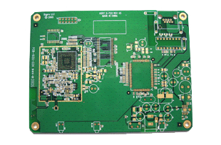
Professional PCB manufacturing and assembly
Building 6, Zone 3, Yuekang Road,Bao'an District, Shenzhen, China
+86-13410863085Mon.-Sat.08:00-20:00

1. It is recommended that you involve your EMS partners as soon as possible. It is better to leave enough time for prototype design and trial production when your PCB layout draft is available. For all the checks you perform on paper or on your PC, there may be some "features" that are displayed only when you produce the first batch of products. These components need to be refreshed before ordering all components for your first planned production build and submitting the design for CE certification.
2. Incorrect PCB panel
The ideal panel depends on the process that the PCB and components will go through. If it is too large or too small, it may not be suitable for the production line. Particularly thin PCBs (e.g. 0.8mm) may need to be in smaller panels to avoid bending. Due to the lack of waste belt, it may be difficult to deal with in production and testing. Breakthrough at the wrong location may mean that the component is not rigid enough, or it is difficult to break through without damaging the component. The absence of a datum point can cause alignment problems. The best practice recommendation is to allow your EMS partners to work with their PCB suppliers to optimize the panel design.
3. Too complex
Unfortunately, if you install SMT on both sides of the component, the cost is higher (usually twice), so do not do this unless you really need it. This also applies to through hole assemblies. Spending more time in the early stages of helps shorten the assembly phase and reduce costs.
4. Wrong part size or shape size
It is worth carefully checking whether the PCB components you specify on the bill of materials (BOM) are actually applicable to the pads of PCB design. Also consider whether the main body of the component is suitable; Generally, components are placed too close or too close to the edge of the PCB, which may cause them to be damaged during disconnection or processing.
5. Through hole in the pad
This is tempting when space is tight, but to avoid solder disappearing from the hole when trying to connect components, the through hole needs to be sealed.
6. Too many component types
Number of components.
7. Dimension of mixing parts
As micro components become more common, they are easy to use, but if they are placed next to larger components that require more solder paste, the process becomes a bit tricky and may require more expensive step templates. This is not a good idea.
8. Improper surface treatment of printed circuit board
HASL according to ROHS standard is usually specified as standard surface treatment, but it is not applicable to fine pitch parts. The shelf life of silver veneer is shorter than that of most products - maybe ENIG is enough? Consider whether the originally listed surface is the most suitable one and how to change it to another surface, which can save time and cost in the assembly phase.
9. Unnecessary components
When you go beyond prototyping, do you really need these test points or programming heads? Obviously, removing them will reduce ongoing costs.
10. Lack of resistance
PCB components may easily share pads, or leave solder resist between pads on equipment with small spacing. Try to consider the location of solder flow, as well as the cost of failure and rework in case of unnecessary short circuit.


Just upload Gerber files, BOM files and design files, and the KINGFORD team will provide a complete quotation within 24h.