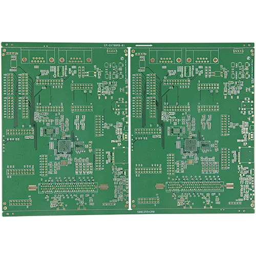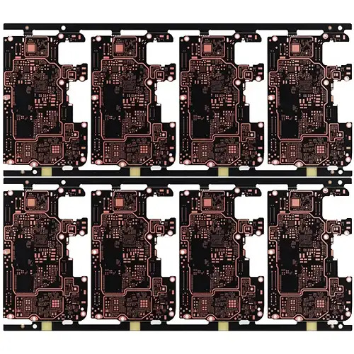
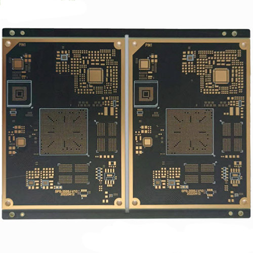
10-layer 1-level HDI PCB
Name: 10-layer 1-level HDI pcb
Layers: 1+8+1
Sheet: FR4 Tg170
Plate thickness: 1.6mm
Panel size: 121.6*95mm/2
Outer copper thickness: 1OZ
Inner layer copper thickness: 1OZ
Minimum through hole: 0.20mm
Minimum blind hole: 0.10mm
Minimum BGA: 0.25mm
Line width line spacing: 3/2.7mil
Surface Treatment: Immersion Gold 2μ''
Blind hole process: hole filling and electroplating
Technical features:
50 Ω Antenna, 90Ω & 100Ω Differential Impedance
application:
Cell Phones, Tablets, Ultrabooks, E-Readers, MP3 Players, GPS, Portable Game Consoles, DSCs, Cameras, LCD TVs, POS Terminals
HDI PCBs are widely used to reduce the weight and overall size of products, as well as improve the electrical performance of devices. High-density PCBs are often found in mobile phones, touch screen devices, laptops, digital cameras, and 4G network communications. HDI PCB also plays an important role in medical equipment as well as various electronic aircraft components. The possibilities for high-density interconnect PCB technology seem almost limitless.
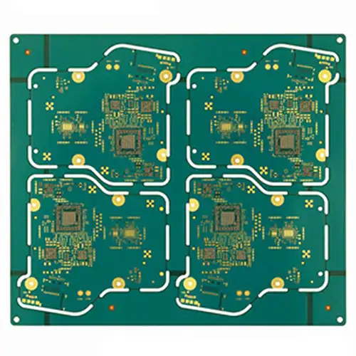
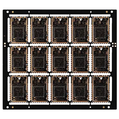
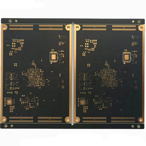
Name: 10-layer 1-level HDI pcb
Layers: 1+8+1
Sheet: FR4 Tg170
Plate thickness: 1.6mm
Panel size: 121.6*95mm/2
Outer copper thickness: 1OZ
Inner layer copper thickness: 1OZ
Minimum through hole: 0.20mm
Minimum blind hole: 0.10mm
Minimum BGA: 0.25mm
Line width line spacing: 3/2.7mil
Surface Treatment: Immersion Gold 2μ''
Blind hole process: hole filling and electroplating
- Previous:2+N+2 HDI ITEQ PCB 6L PCB
- Next:10-layer 3-stage HDI PCB