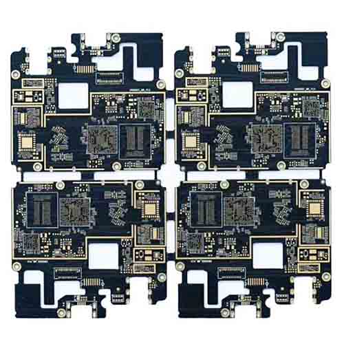
6L 2+N+2 HDI Communication PCB
Name: 6L 2+N+2 HDI Communication PCB
Model : 2+N+2 HDI Communication PCB
Layers : 6Layers
Material: IT150
Construction : 2+2+2 HDI PCB
Finished Thickness: 0.8mm
Copper Thickness: 0.5OZ
Color : Green/White
Surface Treatment: Immersion Gold+OSP
Min Trace / Space: 3mil/3mil
Min Hole: Laser Hole 0.1mm
Application : Communication HDI PCB
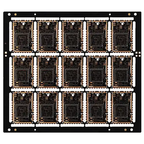
HDI PCB (2+N+2)
Features:
For BGAs with smaller ball pitch and higher I/O count
Increase routing density in complex designs
Sheet Capability
Lower Dk/Df material for better signal transmission performance
copper filled vias
Applications: Mobile phones, PDAs, UMPCs, portable game consoles, digital cameras, camcorders
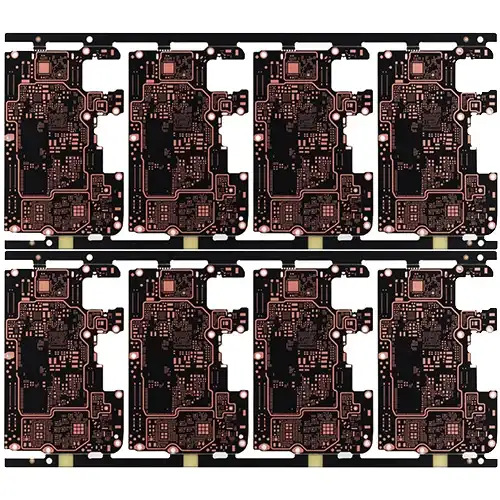
Name: 6L 2+N+2 HDI Communication PCB
Model : 2+N+2 HDI Communication PCB
Layers : 6Layers
Material: IT150
Construction : 2+2+2 HDI PCB
Finished Thickness: 0.8mm
Copper Thickness: 0.5OZ
Color : Green/White
Surface Treatment: Immersion Gold+OSP
Min Trace / Space: 3mil/3mil
Min Hole: Laser Hole 0.1mm
Application : Communication HDI PCB