
Professional PCB manufacturing and assembly
Building 6, Zone 3, Yuekang Road,Bao'an District, Shenzhen, China
+86-13410863085Mon.-Sat.08:00-20:00

The professional pcb design company will give you some PCB wiring principles here. Usually, we should do the following rules
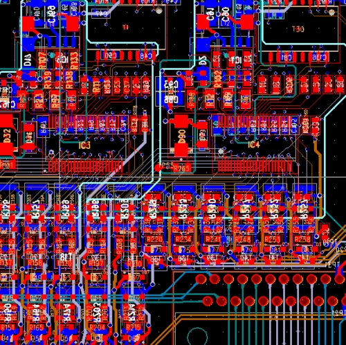
1.1 Digital, analog and DAA (data access arrangement) signal wiring areas are pre divided on PCB.
1.2 Digital and analog PCB components and corresponding wiring shall be separated as far as possible and placed in their respective wiring areas.
1.3 The high-speed digital signal wiring shall be as short as possible.
1.4 The sensitive analog signal wiring shall be as short as possible.
1.5 Reasonably distribute power and ground.
1.6 DGND, AGND and field separation.
1.7 Wide wires shall be used for power supply and critical signal wiring.
1.8 The digital circuit is placed near the parallel bus/serial DTE interface, and the DAA circuit is placed near the telephone line interface.
2. Component placement
2.1 In the system circuit schematic diagram, professional pcb design companies:
a) Divide digital, analog, DAA circuits and related circuits;
b) Divide digital, analog and mixed digital/analog components in each circuit;
c) Pay attention to the positioning of power supply and signal pins of each IC chip.
2.2 The wiring area of digital, analog and DAA circuits on the PCB board is preliminarily divided (generally 2/1/1), and the digital, analog components and their corresponding wiring are as far away from and limited in their respective wiring areas as possible.
Note: When DAA circuit accounts for a large proportion, there will be more control/status signal wiring going through its wiring area, which can be adjusted according to local rules, such as component spacing, high voltage suppression, current limitation, etc. www.pcbdown.cn
2.3 After preliminary division, place components from Connector and Jack:
a) The location of plug-ins shall be reserved around the connector and jack;
b) Space for power supply and ground wiring shall be reserved around components;
c) The location of corresponding plug-ins shall be reserved around the socket.
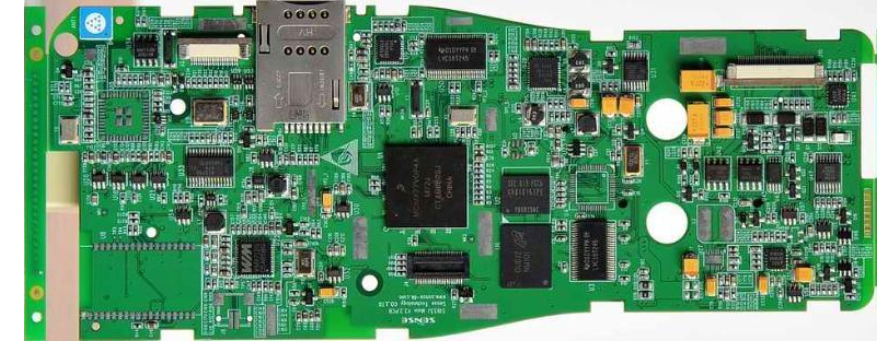
2.4 First place hybrid PCB components (such as Modem devices, A/D, D/A conversion chips, etc.):
a) Determine the placement direction of components, and try to make the digital signal and analog signal pins face the respective wiring area;PCB side
b) Place components at the junction of digital and analog signal wiring areas.
2.5 Place all simulators:
a) Place analog circuit components, including DAA circuit;
b) Simulators are close to each other and placed on the containing TXA1, TXA2, RIN, VC, VREF signal wiring;
c) Avoid placing high noise components around TXA1, TXA2, RIN, VC, VREF signal wiring;
d) For serial DTE modules, DTE EIA/TIA-232-E
The receiver/driver of serial interface signals shall be as close to the connector as possible and far away from the high frequency clock signal wiring to reduce/avoid the added noise suppression devices on each line, such as choke coils and capacitors.
2.6 Professional pcb design companies place digital components and decoupling capacitors:
a) Digital components are placed in a centralized manner to reduce the length of wiring;
b) Place a 0.1uF decoupling capacitor between the power supply/ground of the IC, and keep the connection wires as short as possible to reduce EMI;
c) For parallel bus module, components are close to each other
The connector is placed on the edge to meet the application bus interface standard, for example, the ISA bus routing length is limited to 2.5 inches;
d) For the serial DTE module, the interface circuit is close to the connector;
e) The crystal oscillator circuit board shall be as close to its driver as possible.
2.7 The ground wires of each area are usually connected at one or more points with 0 Ohm resistors or beans.
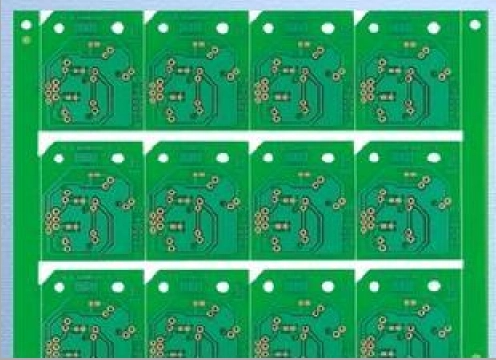


Just upload Gerber files, BOM files and design files, and the KINGFORD team will provide a complete quotation within 24h.