
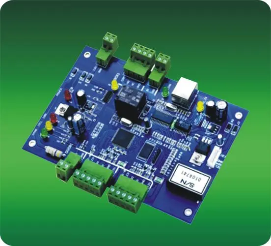
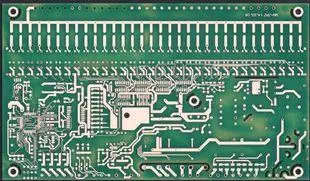
Professional PCB manufacturing and assembly
Building 6, Zone 3, Yuekang Road,Bao'an District, Shenzhen, China
+86-13410863085Mon.-Sat.08:00-20:00

1。 How to choose pcb board design?
The selection of pcb board design must achieve a balance between meeting the design requirements and the PCB production and cost of large models. The design requirements include two parts: electrical and institutional. When designing ultrahigh speed printed PCB boards (with frequencies greater than GHz), this material problem is usually more important. For example, the FR-4 material commonly used today has a great impact on signal attenuation due to its dielectric loss at a frequency of several thousand MHz, which may not be applicable. As far as electricity is concerned, attention should be paid to whether the dielectric constant and dielectric loss are suitable for the design frequency.
2。 How to avoid high-frequency interference?
The basic idea to avoid high-frequency interference is to minimize the interference of high-frequency signal electromagnetic field, which is called crosstalk. You can widen the distance between high-speed signal and analog signal, or add ground protection/shuttle beside analog signal. Attention should also be paid to the noise interference from digital ground to analog ground.
3。 How to solve the signal integrity problem in high-speed design?
Signal integrity is basically a problem of PCB impedance matching. Factors affecting impedance matching include signal source structure and output impedance, routing characteristic impedance, load terminal characteristics, routing topology, etc. The solution is to terminate and adjust the routing topology.
4。 How is the difference distribution line realized?
There are two points to note in differential pair routing. First, the length of the two lines should be as long as possible. The other is that the distance between two lines (determined by differential impedance) should be kept constant, that is, parallel. There are two parallel ways. One is that two lines walk on the same line side by side, and the other is that two lines walk on adjacent layers (up and down). Generally, the former is implemented in multiple ways in parallel.
5。 How to realize the difference distribution line of single output clock signal line?
Only when the signal source and receiver are differential signals, it is meaningful to use differential distribution lines. Therefore, the difference distribution line cannot be used for clock signals with only one output?
6。 Can matching resistors be added between differential pairs at the receiving end?
The matching resistance between differential line pairs at the receiving end is usually added, and its value should be equal to the differential impedance value. In this way, the signal quality will be better.
7。 Why should the wiring of differential pairs be tight and parallel?
The wiring of differential pairs should be properly closed and parallel. Is the so-called appropriate method because this spacing will affect the difference? The value of differential impedance is an important parameter for designing differential pairs. In order to maintain the consistency of differential impedance, parallelism is also required. If the two lines are far or near, the differential impedance will be inconsistent, which will affect signal integrity and timing delay.
8。 How to deal with some theoretical conflicts in actual PCB routing
1。 Basically, the division and isolation of analog/digital is correct. It should be noted that the signal route should not cross the moat as much as possible, and the return current path of power and signal should not become too large.
2。 Crystal oscillator is an analog positive feedback oscillator. In order to obtain stable oscillation signal, the specifications of loop gain and phase must be met. The oscillation specification of the analog signal is easy to be interfered. Even if the grounding protection wiring is added, the interference may not be completely isolated. In addition, if the distance is too far, the noise on the ground plane will also affect the positive feedback oscillation circuit. Therefore, the distance between the crystal oscillator and the chip must be kept as close as possible.
3。 Admittedly, there are many conflicts between high-speed PCB wiring and electromagnetic interference requirements. However, the basic principle is that some electrical characteristics of the signal do not conform to the specifications due to the increased resistance and capacitance caused by electromagnetic interference or ferrite beads. Therefore, it is better to solve or reduce the electromagnetic interference problem by arranging the wiring and designing the laminate of the pcb board. For example, the internal high-speed signal wiring. Finally, use resistance capacitors or ferrite beads to reduce the damage to the signal.
9。 How to solve the contradiction between manual wiring and automatic wiring of high-speed signals?
Most automatic routers with more powerful routing software now set limits on the routing method and the number of vias. The winding engine capability and constraint setting items of each EDA company sometimes vary greatly. For example, whether there are enough constraints to control the serpentine path, whether the trace spacing of the differential pair can be controlled, and so on. This will affect whether the routing method of automatic routing conforms to the designer's idea. In addition, the difficulty of manually adjusting the wiring is absolutely related to the ability of the winding engine. For example, the propelling ability of the trace, the propelling ability of the through-hole, and even the propelling ability of the trace to the copper coating. Therefore, the solution is to choose a wiring device with strong winding engine capability.
10. About test piece
The test sample is used to measure whether the characteristic impedance of the pcb board designed for production meets the design requirements of the time domain reflectometer. Generally, the impedance to be controlled includes single line and differential pair. Therefore, the line width and distance (band differential pair) of the trace on the test sample should be the same as those to be controlled. The most important is the location of the grounding point during the measurement. In order to reduce the inductance of the grounding lead, the grounding position of the TDR probe is usually very close to the signal measurement position (probe tip), so the distance and mode between the signal measurement point and the grounding point on the test sample should be consistent with the probe used.


Just upload Gerber files, BOM files and design files, and the KINGFORD team will provide a complete quotation within 24h.