
Professional PCB manufacturing and assembly
Building 6, Zone 3, Yuekang Road,Bao'an District, Shenzhen, China
+86-13410863085Mon.-Sat.08:00-20:00

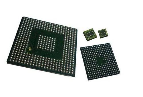
BGA package introduction
BGA package (Ball Grid Array Package), that is, ball grid array, is a surface mount package chip used for an integrated circuit. Xiaoliu, I was a little confused at the beginning, what the hell is a ball grid array? In fact, it is an auxiliary equipment used in BGA soldering technology. The grid is the grid, which is used to position the BGA pins on the PCB pad; the ball is the solder ball, or solder paste, and the solder ball is placed on the solder pad. On the plate, it is called planting balls. The pins are ball-shaped and arranged in a grid-like pattern, hence the name BGA.
When it comes to BGA packaging, we must talk about its advantages:
1. Small size and large memory, the same memory product with the same capacity, the volume is only one-third of the TSOP package.
2. The pins of the previous package form are distributed around. When there are many pins, the spacing is reduced to a certain extent, and the pins are easy to deform. However, the BGA solder balls are at the bottom of the package, and the spacing increases instead, which greatly improves the yield.
3. Good electrical performance. The BGA pins are very short, and solder balls are used instead of leads, which makes the signal path short, reduces lead inductance and capacitance, and enhances electrical performance.
4. Good heat dissipation. The contact surface between the spherical contact array and the substrate is large and short, which is good for heat dissipation.
5. Good coplanarity, high reliability!
The emergence of BGA packaging has become the best choice for high-density, high-performance, multi-pin packaging such as CPUs and south/north bridge chips on motherboards.
Device placement
The accurate placement of BGA depends largely on the accuracy of the placement machine and the recognition ability of the image recognition system. At present, the accuracy of various placement machines on the market has reached about 0.001mm. In addition, because BGA devices have the ability to automatically arrange and position during the reflow soldering process, 50% of the placement accuracy error is allowed, so in the placement accuracy There will be no problem. As long as the BGA device is recognized by the image, it can be accurately mounted on the printed circuit board. Sometimes the BGA identified by the mirror image is not a 100% device with good solder balls, and it is possible that a certain solder ball is slightly smaller than other solder balls in the Z direction. In order to ensure good soldering, it is usually possible to reduce the thickness of the BGA device by 25.41-50.80 μm, and at the same time use a delay to turn off the vacuum system for about 400ms, so that the solder balls of the BGA device can fully contact with the solder paste during placement, reducing the BGA part. The phenomenon of pin virtual soldering. For μBGA and CSP, the above method cannot be used to prevent bad soldering phenomena such as bridging.
Component placement and positioning
The CCGA with a smaller form factor can determine the center position of the component through the outer frame of the ceramic chip. The appearance positioning line is designed on the PCB, the line width is generally 0.2-0.25mm, as shown in the figure, it is used for positioning during placement. Another alignment method is to align according to the welding post array, that is, according to the center position of the welding post array.
3.3 BGA reflow soldering process
When designing the PCB before soldering, the pad design of all solder joints of the BGA needs to be the same size. In addition, due to many soldering failures caused by unqualified solder mask, it is necessary to check whether the solder mask around the pad is qualified before soldering. The vias around the pads on the soldering surface must be coated with a solder resist film. The purpose is to prevent air from entering from below to form a cavity during soldering, and to prevent solder from flowing out of the through holes during soldering.
eflow soldering is the most difficult step in the BGA assembly process, so obtaining a better reflow curve is the key to getting a good BGA soldering. During the welding process, it is necessary to ensure that the welding curve is smooth and the device is heated evenly, especially in the welding area, to ensure that all solder joints are fully melted.
When measuring the temperature curve of reflow soldering, the measurement point should be between the BGA pin and the circuit board. Try not to use high-temperature tape for the temperature measurement probe, but use high-temperature solder paste for welding and fix the thermocouple to ensure a more accurate curve. data. In terms of temperature uniformity, it is necessary to ensure that the temperature difference between the surface of the component, the solder joint and the bottom of the PCB is less than 10°C.
(1) Preheating stage
During this period of time, the PCB is evenly heated and the flux is activated. Generally, the heating speed should not be too fast, and should be controlled below 3°C/s to prevent the PCB from being heated too fast and causing large deformation. The ideal heating rate is 2°C/s, and the time is controlled between 60 and 90 seconds.
2) Infiltration stage
At this stage, the flux begins to volatilize. The temperature should be maintained between 150°C and 180°C for 60 to 120 seconds, so that the flux can fully play its role. The heating rate is generally 0.3 ~ 0.5 ℃ / s.
(3) Reflow stage
The temperature at this stage has exceeded the melting point temperature of the solder paste, the solder paste melts into a liquid, and the component pins are tinned. In this stage, the time when the temperature is above the melting point should be controlled between 60 and 90 seconds. If the time is too little or too long, it will cause welding quality problems. Among them, the time control of the temperature within the peak range is quite critical, and it is generally best to control it within 10 to 20 seconds.
(4) Cooling stage
At this stage, the solder paste begins to solidify and the components are fixed on the circuit board. The cooling rate should not be too fast, generally controlled below 4°C/s, and the ideal cooling rate is 3°C/s. Too fast cooling rate will cause cold deformation of the circuit board, causing quality problems of BGA soldering, especially the false soldering of BGA outer ring pins.
3.7 BGA post-soldering inspection
BGA technology changes the "J"-shaped or wing-shaped leads of the original device PLCC/QFP package into ball-shaped leads; changes the "single-linear" lead-out leads from the device body around the body to the "full-plane" type under the belly of the body. grid array arrangement. This can not only evacuate the pin spacing, but also increase the number of pins. After BGA soldering, the solder joints are hidden under the package. It is necessary to understand and test the physical factors that affect its long-term working reliability, such as the amount of solder, the positioning of wires and pads, and wettability. It is impossible to 100% visually inspect the surface mount. welding quality. At present, the methods for controlling the quality of the assembly process and identifying defects in BGA device assembly mainly include optical inspection, electrical inspection, boundary scan and X-ray inspection.
The use of ball grid arrays (BGAs) and other area array devices is quickly becoming standard in modern PCB design. Many electronics assembly manufacturers face an inspection challenge: ensuring correct assembly and process yield, and traditional verification methods are no longer sufficient. Today, more and more manufacturers are choosing X-rays for their inspection requirements. By using X-ray inspection, the characteristics of hidden solder joints of BGA, micro BGA and flip-chip components can be checked out early in the production run in a reliable and non-destructive manner. Also, most personnel can make pass/fail decisions.
Most PCB manufacturers do not use X-ray systems in their inspection process until BGAs are used in product designs. Traditional methods, such as automated optical inspection (AOI, automated optical inspection), manual visual inspection, electrical testing including manufacturing defect analysis (MDA, manufacturing defect analysis), and in-circuit and functional testing, are used to test PCB components. However, these methods do not provide accurate inspection of hidden soldering problems such as voids, cold welds, and poor solder adhesion. X-ray inspection is effective in finding such problems, monitoring quality assurance and providing immediate feedback for process control.
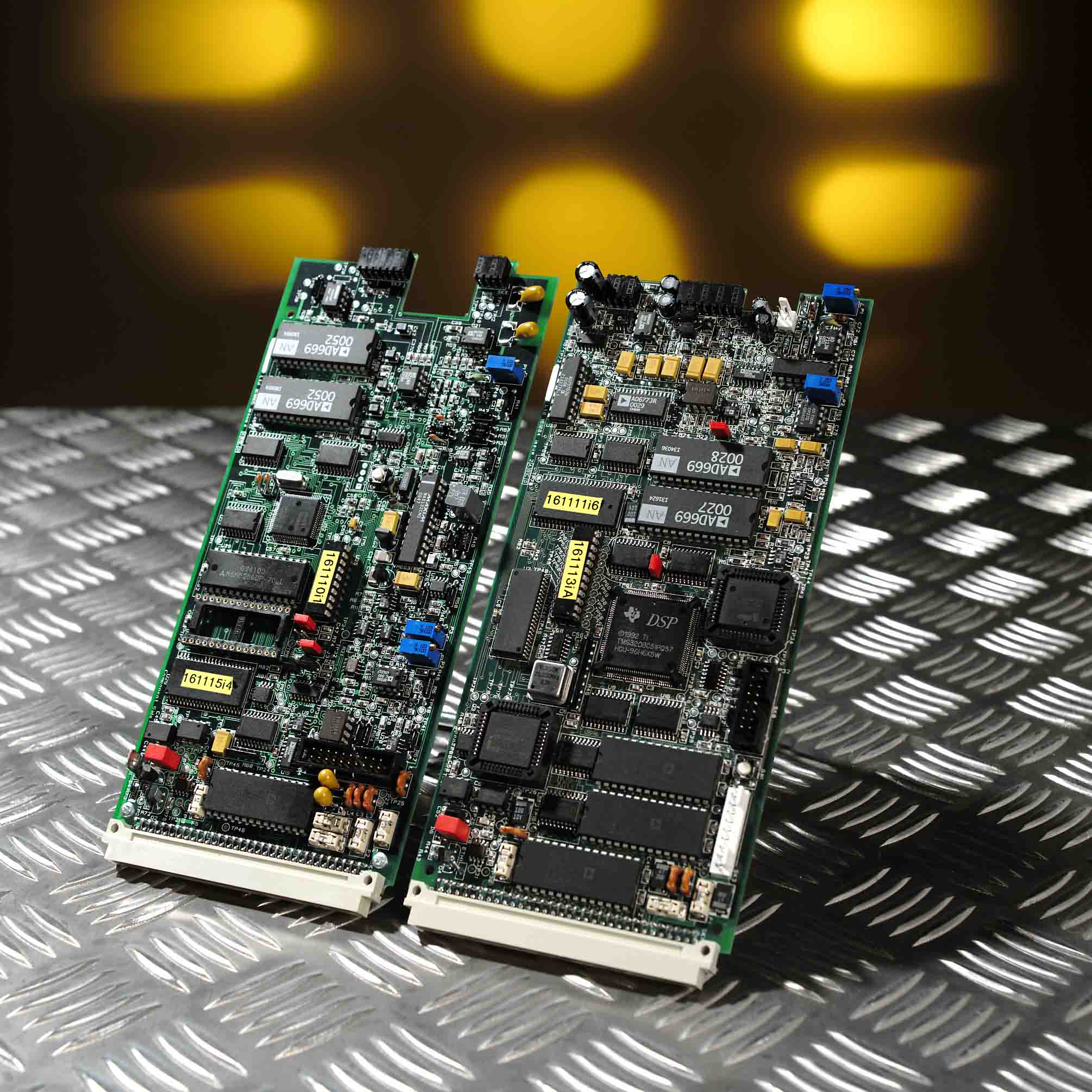
BGA component assembly
Jun 05,2023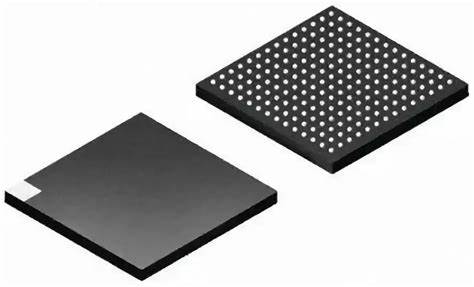


Just upload Gerber files, BOM files and design files, and the KINGFORD team will provide a complete quotation within 24h.