
Professional PCB manufacturing and assembly
Building 6, Zone 3, Yuekang Road,Bao'an District, Shenzhen, China
+86-13410863085Mon.-Sat.08:00-20:00

In the design of any switching power supply, the physical design of PCB board is the last link. If the design method is not proper, PCB may radiate excessive electromagnetic interference, resulting in unstable power supply. The following is an analysis of the matters that need attention in each step:
First, from schematic to PCB design process to establish component parameters -> Input principle netsheet -> Design parameter setting -> Manual layout -> Manual wiring -> Verify the design -> review CAM output.
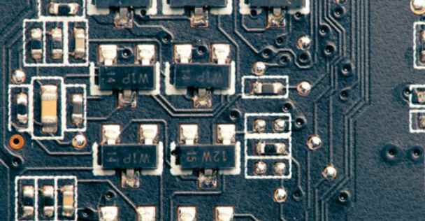
The spacing between adjacent wires must meet the electrical safety requirements, and in order to facilitate operation and production, the spacing should also be as wide as possible. When the wiring density is low, the distance between signal lines can be increased appropriately. For signal lines with a wide gap between high and low levels, the distance should be shortened and increased as far as possible. In general, the distance between lines should be set to 8mil. The distance between the inner hole edge of the pad and the printed board edge should be greater than 1mm, so as to avoid the defects of the pad during processing. When the wire connection with the pad is fine, the connection between the pad and the wire should be designed into a droplet shape. The advantage of this is that the pad is not easy to peel, but the wire and the pad are not easy to disconnect.
Practice has proved that even if the circuit schematic design is correct and the printed circuit board is improperly designed, the reliability of electronic equipment will be adversely affected. For example, if two thin parallel lines on a printed board are close together, there will be a delay in the signal waveform, resulting in reflected noise at the end of the transmission line; Due to the interference caused by the inconsiderate power supply and ground wire, the performance of the product will decline, therefore, in the design of printed circuit board, should pay attention to the correct method.
Each switching power supply has four current circuits:
(1) AC circuit of power switch
(2) Output rectified AC circuit
(3) Input signal source current circuit
(4) Output load current loop the input loop charges the input capacitor through an approximate DC current, and the filter capacitor mainly plays a role of broadband energy storage; Similarly, output filter capacitors are used to store high-frequency energy from the output rectifier while eliminating DC energy from the output load loop. Therefore, the terminals of the input and output filter capacitors are very important. The input and output current loops should be connected to the power supply only from the terminals of the filter capacitors. If the connection between the input/output loop and the power switch/rectifier loop cannot be directly connected to the terminal of the capacitor, AC energy will be filtered by the input or output capacitor and radiated into the environment. The AC circuits of the power switch AC circuit and the rectifier AC circuit contain high amplitude trapezoidal current. These currents have a high harmonic component and their frequency is much higher than the switching fundamental frequency. The peak amplitude can be up to 5 times that of the continuous input/output DC current amplitude. These two circuits are the most likely to produce electromagnetic interference, so they must be laid before other printed wires in the power supply. The three main components of each circuit, the filter capacitor, the power switch or rectifier, the inductor or the transformer, should be placed next to each other, and the position of the components should be adjusted to make the current path between them as short as possible. The best way to establish a switching power supply layout is similar to its electrical design. The best design process is as follows:

Placement transformer
Design the power switch current loop
Design the output rectifier current loop
A control circuit connected to an AC power circuit
Design input current source loop and input filter Design output load loop and output filter according to the functional unit of the circuit, the layout of all components of the circuit, to comply with the following principles:
(1) The size of PCB should be considered first. When PCB size is too large, the printed line is long, the impedance increases, the anti-noise ability decreases, and the cost increases. Too small, the heat dissipation is not good, and the adjacent lines are susceptible to interference. The best shape of the circuit board is rectangular, the aspect ratio is 3:2 or 4:3, and the components located on the edge of the board are generally not less than 2mm away from the edge of the board.
(2) When placing the device, the future welding should be considered, not too intensive.
(3) Take the core component of each functional circuit as the center, and carry out the layout around it. The components should be arranged evenly, neatly and compact on the PCB, and the leads and connections between the components should be reduced and shortened as far as possible. The decoupling capacitor should be as close to the VCC of the device as possible.
(4) For circuits working at high frequency, distribution parameters between components should be considered. General circuits should be arranged as parallel as possible. In this way, not only beautiful, but also easy to assemble welding, easy to mass production.
(5) Arrange the position of each functional circuit unit according to the circuit flow, so that the layout is convenient for signal flow, and keep the signal in the same direction as far as possible.
(6) The first principle of layout is to ensure the distribution rate of wiring, mobile devices pay attention to the connection of the fly line, and put the connected devices together.
(7) Reduce the area of loop as much as possible to suppress the radiation interference of switching power supply
Eight kinds of PCB surface treatment technology
Apr 03,2023


Just upload Gerber files, BOM files and design files, and the KINGFORD team will provide a complete quotation within 24h.