
Professional PCB manufacturing and assembly
Building 6, Zone 3, Yuekang Road,Bao'an District, Shenzhen, China
+86-13410863085Mon.-Sat.08:00-20:00

With the continuous improvement of human requirements for living environment, the environmental problems involved in PCB production are particularly prominent. The topic of lead and bromine is the hottest, lead-free and halogen-free will affect the development of PCB in many ways.
Although at present, the changes in PCB surface treatment process are not very big and seem to be a relatively distant thing, it should be noted that long term slow changes will lead to great changes. In the case of environmental protection increasingly loud voice, PCB surface treatment technology will definitely change in the future.
The most basic purpose of surface treatment is to ensure good solderability or electrical properties. Since natural copper tends to exist in the form of oxides in the air, it is unlikely to remain as raw copper for a long time, so other treatments are required for copper. Although strong flux can be used to remove most copper oxides in subsequent assembly, strong flux itself is not easily removed, so it is generally not used in the industry.
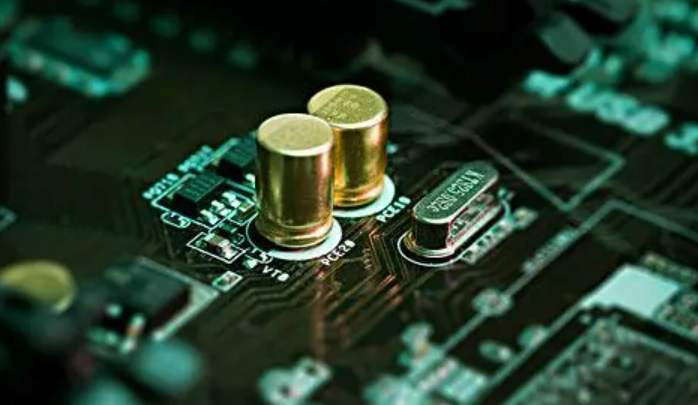
There are many PCB surface treatment processes. The common ones are hot air finishing, organic coating, electroless nickel plating/gold dipping, silver dipping and tin dipping, which are described below.

1, hot air leveling (spray tin)
Hot air leveling, also known as hot air solder leveling (commonly known as tin spray), is a process of coating molten tin (lead) solder on the surface of PCB and heating compressed air leveling (blowing), so that it forms a layer of copper oxidation resistance, and can provide good solderability of the coating. Hot air conditioning solder and copper at the joint of the formation of copper tin gold compounds. PCB for hot air polishing usually to sink in the molten solder; The air knife blows out the liquid solder before it sets; The air knife minimizes the meniscus of solder on the copper surface and prevents solder bridging.
2, organic weldability protection agent (OSP)
OSP is printed circuit board (PCB) copper foil surface treatment in line with the RoHS directive requirements of a process. OSP is short for Organic Solderability Preservatives, also known as organic solderability preservatives and Preflux in English. Simply put, OSP is a chemically grown organic skin film on a clean, bare copper surface.
This layer of film has anti-oxidation, heat shock, moisture resistance, to protect the surface of copper in the normal environment no longer continue to rust (oxidation or vulcanization, etc.); But in the subsequent welding high temperature, this protective film must be easily removed by the flux quickly, so that the exposed clean copper surface can be immediately combined with the molten solder in a very short time to become a solid solder spot.
3, full plate nickel plating gold
Nickel plating is a process in which the PCB surface conductor is first coated with a layer of nickel and then coated with a layer of gold. Nickel plating is mainly to prevent the diffusion between gold and copper. There are two types of electroplated nickel gold: soft gold plating (pure gold, the surface of gold does not look bright) and hard gold plating (smooth and hard surface, wear-resistant, containing cobalt and other elements, the surface of gold looks brighter). Soft gold is mainly used in chip packaging gold wire; Hard gold is mainly used for electrical interconnection in non-welded places.
4. Sink gold
Gold plating is a thick layer of good electrical nickel gold alloy on the copper surface, which can protect the PCB for a long time; In addition, it has environmental tolerance that other surface treatment processes do not have. Sinking gold also prevents copper from dissolving, which would help lead-free assembly.
5. Sinking tin
Since all solder is currently based on tin, the tin layer can be matched to any type of solder. Tin sinking process can form flat copper-tin intermetallic compounds. This property makes tin sinking have the same good solderability as hot air leveling without the headache flat problem of hot air leveling. The tin plate cannot be stored for too long and must be assembled according to the order of the tin sinking.
6. Sink silver
Silver plating process is between organic coating and electroless nickel plating/gold plating, which is relatively simple and fast. Even when exposed to heat, humidity, and pollution, silver is still able to maintain good solderability, but tarnish. Silver plating does not have the good physical strength of electroless nickel/gold plating because there is no nickel underneath the silver layer.
7. Chemical nickel palladium
Compared with gold precipitation, there is an extra layer of palladium between nickel and gold. Palladium can prevent the corrosion caused by replacement reaction and make full preparation for gold precipitation. Gold is closely coated with palladium, providing a good contact surface.
8. Electroplating hard gold
In order to improve the wear resistance of the product, increase the number of insertion and removal of hard gold plating.
With more and more high requirements of users, environmental requirements are more and more strict, surface treatment process is more and more, in the end the choice of the kind of development prospects, more universal surface treatment process, seems to be a little dazzling, confusing. It is impossible to predict exactly where PCB surface treatment technology will go in the future. Anyway, to meet the requirements of users and protect the environment must be done first!


Just upload Gerber files, BOM files and design files, and the KINGFORD team will provide a complete quotation within 24h.