
Professional PCB manufacturing and assembly
Building 6, Zone 3, Yuekang Road,Bao'an District, Shenzhen, China
+86-13410863085Mon.-Sat.08:00-20:00

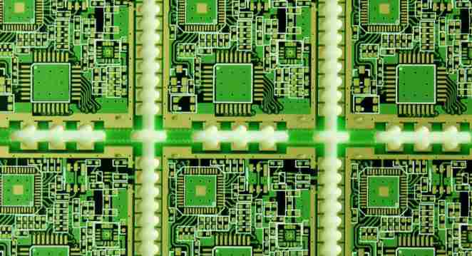
FPC Flexible Printed Circuit (FPC Flexible Printed Circuit) is a form of circuit made in a flexible printed surface, with or without a overlay (usually used to protect FPC circuits). Because FPC can bend, fold or repeat in a variety of ways, it has advantages such as light, thin and flexible compared to ordinary hard board (PCB), so it is being used more and more widely.
FPC (Base Film) materials generally use Polyimide (PI), also useful polyester
(Polyester (PET) : Material thickness: 12.5/25/50/75/125um (12.5 and 25um are commonly used). If FPC needs to be welded at high temperature, its material is usually PI, and PCB substrate is usually FR4.
The Cover Layer of FPC is made of dielectric film and adhesive, or the coating of flexible medium, which has the protective effect of avoiding contamination, dampness, scratches and so on. The main material is consistent with the base material, namely polyimide
(Polyimide) and Polyester (Polyester), common material thickness is 12.5um.
FPC adhesives are used to bond the layers when the FPC is designed. Commonly used flexible board adhesives include Acrylic, Modified Epoxy, Phenolic Butyrals, reinforced adhesives, and pressure sensitive adhesives, while single-layer FPC need not be bonded with adhesives.
In many applications, such as device welding, flexible plates need Stiffener to be stiffened outside. Materials mainly used include PI or Polyester film, glass fiber, polymer material, steel sheet, aluminum sheet, etc. PI or Polyester film is a commonly used material for strengthening flexible boards, with a thickness of 125um. The hardness of glass fiber (FR4) reinforcing board is higher than that of PI or Polyester. It is used in places where the requirements are harder and the processing is difficult.
Compared with the treatment of PCB pad, FPC pad treatment also has a variety of methods, common are as follows:

① Chemical nickel gold is also known as chemical gold leaching or gold sinking. Generally, the thickness of the non-electrolytic nickel layer is 2.5um to 5.0um on the copper surface of the PCB, and the thickness of the gold leaching (99.9% pure gold) layer is 0.05um to 0.1um(the previous news said that a PCB factory workers use the replacement method to replace the gold in the pcb pool). Advantages of the technology: smooth surface, long preservation time, easy to weld; Suitable for fine spaced components and thin thickness PCB. For FPC, it is suitable for use because of its thin thickness. Cons: Not environmentally friendly.
② Advantage of tin-lead Plating: you can directly add flat Lead and Tin to the solder plate, good solderability and uniformity. For some processing processes such as HOTBAR, this method must be used on FPC. Disadvantages: Lead is easy to oxidation, preservation time is short; Electroplating wires need to be drawn; Not environmentally friendly.
③ Selective electroplating (SEG) selective electroplating gold finger PCB local area electroplating with electricity, other areas with another surface treatment. Electroplating refers to the PCB copper surface is coated with nickel layer, after electroplating layer. The thickness of nickel layer is 2.5um-5.0um, and the thickness of gold layer is generally 0.05um-0.1um. Advantages: Thick gold coating, strong oxidation resistance and wear resistance. Goldfinger is usually treated in this way. Disadvantages: not environmentally friendly, cyanide pollution.
(4) Organic weldability protective layer (OSP) This process refers to the surface coating of exposed PCB copper with specific organic matter. Advantages: Can provide a very flat PCB surface, in line with environmental requirements. Suitable for PCB with fine spacing components.
Disadvantages: PCbas requiring conventional and selective wave soldering processes are not allowed to use OSP surface treatment processes.
⑤ Hot air leveling (HASL) The process is to cover the final bare metal surface of the PCB with 63/37 lead tin alloy. The thickness of hot air leveling lead-tin alloy coating is required to be 1um-25um. Hot-air leveling process is difficult to control the thickness of the coating and the pattern of the pad, and is not recommended for PCB with fine-spaced components, because the fine-spaced components have high requirements for the flatness of the pad. Hot air leveling process has great influence on FPC with very thin thickness, so it is not recommended to use this kind of surface treatment.
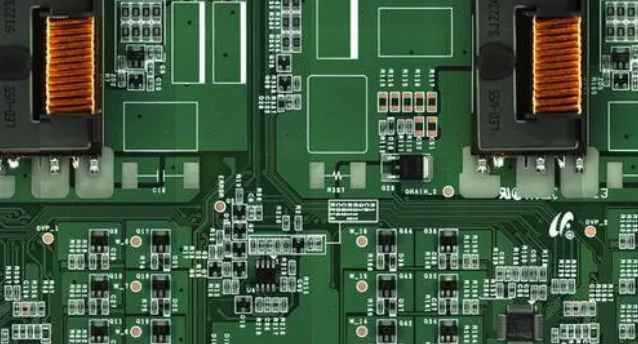
In the design, FPC often needs to be used together with PCB, in the connection of the two usually adopts the board to board connector, connector plus gold finger, HOTBAR, soft and hard combined board, artificial welding way to connect, according to different application environment, designers can use the corresponding connection mode.
In the actual application, according to the application needs to determine whether ESD shielding is needed, when the FPC flexibility requirements are not high, solid copper, thick medium can be used to achieve. When the flexibility requirement is higher, copper mesh and conductive silver paste can be used.
Due to its softness, the FPC is prone to fracture when subjected to stress, so some special means are needed to protect the FPC.


Just upload Gerber files, BOM files and design files, and the KINGFORD team will provide a complete quotation within 24h.