
Professional PCB manufacturing and assembly
Building 6, Zone 3, Yuekang Road,Bao'an District, Shenzhen, China
+86-13410863085Mon.-Sat.08:00-20:00

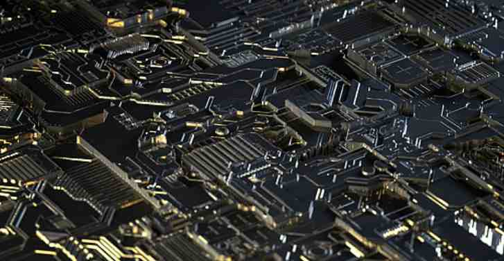
We often compare the crystal oscillator to the heart of the digital circuit, because all the work of the digital circuitis inseparable from the clock signal, and the crystal oscillator directly controls the whole system. If the crystal oscillator does not operate, the whole system will be paralyzed, so the crystal oscillator is a prerequisite for the digital circuit to start working. The crystal oscillator, as we often say, is the quartz crystal oscillator and the quartz crystal resonator. They are made of the piezoelectric effect of the quartz crystal.
Applying an electric field to the two electrodes of a quartz crystal causes a mechanical deformation of the crystal, whereas applying mechanical pressure to either side causes an electric field to occur in the crystal. And both phenomena are reversible. Using this property, alternating voltages are applied to both sides of the crystal, causing the wafer to vibrate mechanically and at the same time generate alternating electric fields. This kind of vibration and electric field are generally small, but at a certain frequency, the amplitude will be significantly increased, which is piezoelectric resonance, similar to the LC loop resonance we commonly see. As the heart of the digital circuit, how does crystal oscillator play a role in smart products?
Smart home such as air conditioning, curtains, security, monitoring and other products, all need wireless transmission module, they through Bluetooth, WIFI or ZIGBEE protocol, the module from one end to the other end, or directly through the mobile phone control, and crystal oscillator is the core component in the wireless module, affecting the stability of the whole system, so choose a good system to use crystal oscillator, Determines the success or failure of digital circuits.
Due to the importance of crystal oscillator in digital circuit, we need to be careful when using and designing:
1. There are quartz crystals inside the crystal oscillator, which is easy to cause quartz crystal breakage and damage when it is impacted or dropped from the outside, thus causing the crystal oscillator to be unable to vibrate. Therefore, the reliable installation of crystal oscillator should be considered in the design of the circuit, and its position should not be close to the plate edge and equipment shell as far as possible.
2. Pay attention to the welding temperature when welding by hand or machine. Crystal vibration is sensitive to temperature, welding temperature should not be too high, and the heating time should be as short as possible. Reasonable crystal distribution can suppress the radiation interference of the system
The product is a field camera, which consists of five parts inside: core control board, sensor board, camera, SD memory card and battery. The shell is plastic and the small board has only two interfaces: DC5V external power interface and USB interface for data transmission. After the radiation test, it is found that the harmonic noise radiation is about 33MHz. The original test data is as follows:

The product shell structure plastic shell, non-shielding material, the whole test only power cord and USB cable out of the shell, is it the interference frequency point is radiated by the power cord and USB cable? Therefore, the following steps are taken to test:
(1) Add magnetic ring only on the power cord, test results: the improvement is not obvious;
(2) Only add magnetic ring on USB cable, test results: the improvement is still not obvious;
(3) Add magnetic ring to both USB cable and power cord, test results: the improvement is obvious, the overall frequency of interference decreased. As can be seen from the above, the interference frequency points are brought out from the two interfaces, which is not the problem of the power interface or USB interface, but the internal interference frequency points coupled to the two interfaces. Shielding only one interface cannot solve the problem. After near field measurement, it is found that a 32.768KHz crystal oscillator from the core control board generates strong spatial radiation, which makes the 32.768KHz harmonic noise coupled to the surrounding wiring and GND, which is then coupled to radiate out through the interface USB cable and power line.
The crystal oscillator's problems are caused by the following two problems:
(1) The crystal vibration is too close to the edge of the plate, which is easy to cause the crystal vibration radiation noise.
(2) There is a signal line under the crystal oscillator, which is easy to cause the harmonic noise of the signal line coupling crystal oscillator. (3) The filter element is placed below the crystal oscillator, and the filter capacitance and matching resistance are not arranged according to the signal direction, which makes the filtering effect of the filter element worse.
Based on the analysis, the following countermeasures are obtained:
(1) The filter capacitance and matching resistance of the crystal are preferentially placed near the CPU chip, far away from the edge of the board; (2) Remember not to lay ground in the crystal placement area and the projection area below;
(2) The filter capacitance and matching resistance of the crystal are arranged in accordance with the signal direction, and placed neatly and compact near the crystal;
(3) The crystal is placed near the chip, and the line between the two is as short and straight as possible. You can refer to the following layout:
After rectification, the prototype test results are as follows:
The clock frequency of crystal oscillators in many systems is high and the interference harmonic energy is strong. Interference harmonics in addition to the input and output of the two lines conducted out, but also from the space radiation, if the layout is not reasonable, easy to cause a strong noise radiation problem, and it is difficult to solve through other methods, so in PCB board layout for crystal oscillator and CLK signal line layout is very important.
Note on PCB design of crystal oscillator
(1) The coupling capacitor should be as close to the power pin of the crystal oscillator as possible. The position should be placed in order: according to the direction of power supply inflow, the capacitor with the smallest capacity should be placed in order from the largest to the smallest capacity. The shell of the crystal oscillator must be grounded, which can radiate the crystal oscillator outwards, and can also shield the interference of external signals on the crystal oscillator.
(2) Do not wire under the crystal oscillator to ensure that the floor is completely covered. At the same time, do not wire within 300mil of the crystal oscillator, so as to prevent the crystal oscillator from interfering with the performance of other wiring, devices and layers.
(3) The route of the clock signal should be as short as possible, the line should be wide, and the balance should be found in the length of the wiring and away from the heat source.
(5) Crystal oscillator should not be placed on the edge of the PCB board, especially in the design of the board card. Statement: This article is reproduced article, reproduced this article for the purpose of transmitting more information, copyright belongs to the original author, if involved in infringement, please contact Xiaobian for processing. (mbbeetchina)


Just upload Gerber files, BOM files and design files, and the KINGFORD team will provide a complete quotation within 24h.