
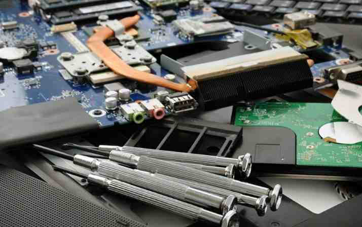
Professional PCB manufacturing and assembly
Building 6, Zone 3, Yuekang Road,Bao'an District, Shenzhen, China
+86-13410863085Mon.-Sat.08:00-20:00

In order to facilitate production, PCB circuit board plate generally needs to design Mark point, V groove, process edge.
First, the shape of the Mosaic
1. The outer frame (clamping edge) of PCB splice board shall adopt closed-loop design to ensure that PCB splice board will not be deformed after fixed on the fixture.
2, PCB board width ≤260mm(SIEMENS line) or ≤300mm(FUJI line); If you need automatic dispensing, PCB board width &TImes; Length ≤125 mm&TImes; 180 mm.
3. PCB board shape should be as close to square as possible, 2&TImes is recommended; 2, 3&TImes; 3. A Mosaic board; But don't spell it as a yin-yang board;
Two, V-shaped slot
After opening V-shaped slot, the remaining thickness X shall be (1/4 ~ 1/3) plate thickness L, but the minimum thickness X shall be ≥0.4mm. The upper limit is recommended for the board with a heavy load, and the lower limit is recommended for the board with a light load.
2. The dislocation S of the upper and lower sides of the V-shaped groove should be less than 0.1mm; Due to the limitation of the minimum effective thickness, it is not suitable to adopt V-slot splice for plates with thickness less than 1.2mm.
Three, Mark point
1. When setting the reference registration point, an open weld area 1.5mm larger than the registration point is usually set aside around it.
2, used to help the optical positioning of the placement machine, there are at least two asymmetric datum points diagonally on the PCB board with the placement device, (copyright all) the whole PCB optical positioning datum points in the corresponding diagonal position of the whole PCB; The reference point for optical positioning of block PCB is generally in the diagonal corresponding position of block PCB board.
3. For QFP(square flat package) with lead spacing ≤0.5mm and BGA(ball grid array package) with ball spacing ≤0.8mm, in order to improve the accuracy of the patch, the reference point is required to be set in the IC diagonal.
Four, the process edge
1. There can be no large devices or protruding devices near the connection point between the outer frame of the splicing board and the inner small board, and the small board and the small board, and the edge of the components and PCB circuit board should be left more than 0.5mm space to ensure the normal operation of the cutting tool.
Five, the plate positioning hole
1. Reference symbol for the positioning of the whole board of PCB circuit board and for the positioning of fine-spaced devices. In principle, QFP with spacing less than 0.65mm should be set in its diagonal position; The positioning reference symbols for PCB subboards shall be used in pairs and arranged diagonally on the positioning elements.
2, large components should have positioning posts or positioning holes, such as I/O interface, microphone, battery interface, micro switch, headphone interface, motor, etc. A good PCB designer, in the plate design, to consider the factors of production, to achieve convenient processing, improve production efficiency, reduce production costs.

Reasonable layout of PCB circuit board components is the basic premise of designing high quality PCB drawings in SMT processing. The requirements of component layout mainly include installation, force, heat, signal and beauty.
1, installation refers to a series of basic requirements put forward in the specific application, in order to smoothly install the circuit board into the case, shell, slot, without space interference, short circuit and other accidents, and make the specified connector in the case or shell on the specified position.
2. In the processing of stress patch, the circuit board should be able to withstand various external forces and vibrations during installation and work. Therefore, the circuit board should have a reasonable shape, and the position of various holes on the board (screw holes, special-shaped holes) should be arranged reasonably. Generally, the distance between the hole and the edge of the plate should be at least larger than the diameter of the hole. At the same time, it should be noted that the weakest section of the plate caused by special-shaped holes should also have enough bending strength. In particular, the connectors that "extend" directly out of the equipment shell on the board should be reasonably fixed to ensure long-term reliability. 3, heat for high-power, serious heating devices, in addition to ensuring heat dissipation conditions, but also pay attention to placing in the appropriate position. Especially in sophisticated analog systems, particular attention should be paid to the adverse effect of the temperature field generated by these devices on the fragile pre-amplifier circuit. Generally, the part with very large power should be made into a separate module, and certain thermal isolation measures should be taken between the signal processing circuit and it.
3, signal signal interference PCB circuit board layout design to consider the most important factor. A few of the most basic aspects are: weak signal circuit and strong signal circuit separation or isolation; The AC part is separated from the DC part; The high-frequency part is separated from the low-frequency part; Pay attention to the direction of the signal line; The arrangement of ground wire; Appropriate screening, filtering and other measures.
4. Beauty should not only consider the orderly placement of components, but also consider the beauty and fluency of the line.
Because the general layman sometimes more emphasis on the former, in order to one-sided evaluation of the merits of circuit design, in order to the image of the product, in the performance requirements are not harsh to give priority to the former. However, in the occasion of high performance, if you have to use dual panels, and the circuit board is packaged inside, usually can not see, you should give priority to emphasize the beauty of the line.
Besides DXP, what software can PCB be drawn? First on our list is the ZentiPCB platform from Mirko Bruno Sortini, which offers a range of free software to help users design their own PCBS.
ZentiCapture allows the user to quickly and easily use a simple functional toolset design schematic, which allows the user to place parts (component symbols) by orthogonal locking and pin capture. Once the schematics (in diagram form) are complete, they can be ported to the ZentiPCb. ZentiPCB is a CAD based program that allows users to import netlist files and visualize their charts. The layout editor provides the ability to import components directly from the library using cursors, with support for single and dual panels depending on your requirements. TinyCAD TinyCAD comes from SourceForge users beischer, don_lucas, and mattpyne. Don't underestimate this software just because of its name. This software provides all the functions of PCB design and wiring design. The software contains 42 libraries of 755 symbols, including digital logic gates, electromechanical components and even microcontrollers. Each component can be edited, and users can even add their own symbols to it. TinyCAD supports a variety of nettables (Eagle SCR, PADS-PCB, XML, etc.) and can also generate SPICE nettables. CometCAD


Just upload Gerber files, BOM files and design files, and the KINGFORD team will provide a complete quotation within 24h.