
Professional PCB manufacturing and assembly
Building 6, Zone 3, Yuekang Road,Bao'an District, Shenzhen, China
+86-13410863085Mon.-Sat.08:00-20:00

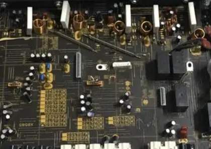
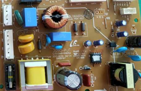
PCBA circuit board can be seen everywhere in our life. Certain flux and impurities will remain on the surface of PCBA welding process. If the PCBA board surface can not effectively ensure cleanliness, it may affect the service life of the product, and even affect the normal operation of the PCBA circuit board. Therefore, in the process of PCBA processing, PCBA cleaning is an essential link, then as a PCBA processing plant, how should we clean PCBA? Next by Shenzhen PCBA processing plant -kingford- with you to share some PCBA cleaning skills, hope to bring you some help!
1. In the water cleaning and semi-water cleaning process, a certain amount of emulsifier can be added to the water. When cleaning synthetic resin by pollutants, these pollutants and emulsifiers emulsify and dissolve in water. The emulsification can be improved by adding surfactant.
2, semi-water cleaning mainly uses organic solvents and deionized water, with a certain amount of active agents, additives composed of cleaning agent. This cleaning is between solvent cleaning and water cleaning. These cleaners are organic solvents, flammable solvents, high flash point, low toxicity, safe to use, but must be rinsed with water and then dried in the oven.
3, water based cleaning agent is a kind of cleaning agent that can be compatible with water. Suitable for water cleaning, some highly concentrated metal cleaning agents can even be diluted with water to 1:10 -- 30, relatively cheap. Due to the principle of high frequency vibration, it can improve the cleaning effect. Usually, it is difficult to clean once or twice, and it needs to be cleaned repeatedly. After cleaning, water spots are easy to remain. However, some products have higher maintenance requirements for the cleaning effect, even in the case of live cleaning and maintenance. If the water-based cleaning agent is used at this time, the internal circuit of the PCBA will be damaged, thus shortening the service life of the product.
4. The most intuitive impact of PCBA pollutants is the appearance of PCBA. If placed or used in a high temperature and humidity environment, there may be residue moisture absorption and whitening phenomenon. Due to the extensive use of leadless chips, microBGA, chip-level packaging (CSP), and 01005 in components, the distance between components and the circuit board is reduced, the size is miniatures, and the assembly density is increasing. If the halide is hidden under the component where it cannot be cleaned, local cleaning may result in catastrophic halide release. PCBA plate cleaning is a process of dissolution and removal of welding residues. The purpose of cleaning is to essentially extend the life of the product by ensuring good surface resistance and preventing leakage.
2. What is wave soldering? Wave soldering process and operation process
Wave soldering is a welding process used in small batch PCBA processing or batch processing. Wave crest welding is to melt solid solder to form liquid through high temperature. After solid solder forms liquid, wave crest is formed on solder groove surface of specific shape with the help of pump. PCBA installed with electronic components infiltrates component pin through wave crest through transmission chain, so that component pin and PCBA welding pad form welding.

Wave soldering process: Insert components into corresponding PCBA through holes → spray flux → preheat (temperature 90-110℃) → wave soldering (240-260℃) → cooling → repair welding → remove pins of excess components → check solder joints.
I. Preparation before wave crest welding
1, open the main switch power supply, according to the equipment use time, through the time solenoid valve control switch tin furnace time;
2. Check whether the temperature indicator of the tin furnace is normal: use a thermometer to measure the temperature about 15mm below the liquid level of the tin furnace, and keep it within the range of ±5℃ with the actual setting temperature;
3. Check the working condition of the foot cutting machine: adjust the height of the blade according to the thickness of the PCPA, requiring the length of the element foot to be 1.4 ~ 2.0mm;
4. Check whether the flux supply is normal: pour the flux, adjust the intake valve, turn on the machine to check whether the flux is foaming or spraying, adjust the flux proportion to meet the requirements;
5, check the tin surface height, if lower than the tin furnace 12-15mm, should be timely add solder, add attention to batch, each batch does not exceed 10kg;
6. Remove tin residue from the tin surface and add anti-oxidant after cleaning;
7, adjust the Angle of the transportation track: according to the width of the PCBA board to be welded, adjust the width of the track, so that the PCBA board by clamping force is moderate. Adjust the track inclination according to the pin density of the welded component.
2, wave soldering boot process
1. Open the flux switch and adjust the thickness of the foam board l / 2 when foaming; When spraying, the board surface is required to be uniform, the spray amount is appropriate, generally not spray component surface is appropriate;
2, adjust the air volume of the air knife, so that the excess flux on the plate drops back to the foaming tank, avoid dropping on the preheater, cause fire;
3. Open the transport switch and adjust the transport speed to the required value;
4. Start the cooling fan.
3. Operation process after wave crest welding
1, close the preheater, tin furnace wave, flux, transport, cooling fan, foot cutting machine and other switches;
2. The flux in the foaming tank needs to be replaced about two weeks after use, and it should be measured regularly during use;
3. After shutdown, the wave machine and chain claw should be cleaned up, and the spray nozzle should be soaked and cleaned with dilution.
Iv. Precautions in wave soldering process
1. The operators must stick to their posts and check the operation of the equipment at any time;
2, the operator should check the quality of the welding plate, such as abnormal welding spot, should immediately stop for inspection;
3. Timely and accurately make the original record of equipment operation and the specific data record of solder joint quality;
The above content is provided by kingford. To learn more about PCBA processing, please visit Shenzhen One Nine Four Two Technology Co., LTD
PCBA board aging test standards and methods
Mar 17,2023


Just upload Gerber files, BOM files and design files, and the KINGFORD team will provide a complete quotation within 24h.