
Professional PCB manufacturing and assembly
Building 6, Zone 3, Yuekang Road,Bao'an District, Shenzhen, China
+86-13410863085Mon.-Sat.08:00-20:00

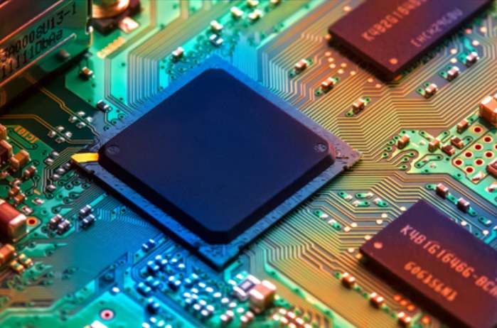
SMT patch processing refers to the process of pasting electronic components and other materials on PCB bare board. It is a popular processing technology in electronic assembly industry. Next, we will give you a detailed introduction to the SMT patch processing process.
One. Preparation before SMT patch processing
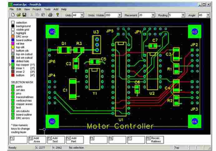
1. Circuit board information (Gerber)
The electronic file of the standard circuit diagram shall include at least 4 layers: PAD file, perforated file, text file and welding proof file;
It would be better if PCB board factory provides connected board Gerber;
Standard plate edge specification: 10mm plate edge is left at the top and bottom;
Standard positioning hole specifications: one positioning hole on the left and right sides of the same plate edge, the center of the circle from both sides of the plate edge 5mm diameter, 4mm round hole;
Standard visual mark point specification: opposite diagonal asymmetrical 1mm solid tinspray round point, outer ring 3mm diameter transparent ring;
2. Material Table (BOM)
The electronic file contains the position coordinates (CAD, text file with extension ".TXT ");
Mixing list of SMT and DIP materials (please provide the part coding principle and the way to distinguish the front and back parts);
SMT front and back materials and DIP materials separate list (please provide the resolution of front and back parts);
SMT front/SMT back/DIP materials separate list.
3. Auxiliary data
Furnace temperature measuring plate (including scrap plate of important parts);
Printed steel plate;
Tow. Detailed SMT patch processing process
1. Material procurement, processing and inspection
According to the customer's BOM list, the material buyer makes the original purchase to ensure the production is correct. After purchasing, inspect and process materials, such as pin arrangement and pin cutting, resistance pin forming, etc. Inspection is to better ensure the quality of production. Novac has specialized suppliers for material procurement, and the upstream and downstream procurement lines are complete and mature.
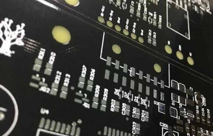
2. Silk screen printing
Screen printing, or screen printing, is the first step in the SMT process. Screen printing refers to the solder paste or patch glue is printed on the circuit board welding pad to prepare for component welding. With the help of a solder paste press, solder paste is permeated through a stainless steel or nickel steel mesh and attached to the pad. If the customer does not provide the steel mesh used for screen printing, the processor needs to make it according to the steel mesh file. At the same time, because the solder paste must be frozen, the solder paste needs to be thawed in advance to the appropriate temperature. The solder paste printing thickness is also related to the scraper. The solder paste printing thickness should be adjusted according to the circuit board processing requirements.
3, dispensing
Generally, in SMT processing, the glue used for dispensing is red glue, which is dropped on the PCB position to fix the components to be welded, so as to prevent electronic components from falling or virtual welding due to self-weight or unfixed reasons during reflow welding. Dispensing can also be divided into manual dispensing or automatic dispensing, according to the need to confirm the process;
4. Mount
Through the functions of suction - displacement - positioning - placing, SMC/SMD components can be quickly and accurately attached to the solder pad position specified by PCB board without damaging the components and printed circuit boards. Mounting is generally located before reflow welding;
5. Curing
Curing is to melt the patch glue, is the surface mount components fixed on the PCB pad, generally using heat curing;
6. Reflow welding
Reflow welding is the soft brazing of mechanical and electrical connections between the welding ends of surface assembled components or pins and the printed board pad by remelting the paste soft brazing material pre-allocated to the printed board pad. It mainly depends on the action of hot gas flow on the solder joint, the gummy flux in a certain high temperature air flow for physical reaction to achieve SMD welding;
7. Cleaning
After the welding process is complete, the panel is cleaned to remove the rosin flux and some of the tin balls to prevent them from short-circuiting between the components. Cleaning is to place the welded PCB board in the cleaning machine to remove the residual flux harmful to human health on the surface of the PCB assembly board or the flux residue after reflow welding and manual welding and the pollutants caused in the assembly process.
8. Detection
Testing is to test the welding quality and assembly quality of the PCB assembly board after assembly. AOI optical detection, flying needle tester and ICT and FCT functional testing are needed. QC team to spot check PCB board quality, detect substrate, flux residue, assembly failure, etc.
9. Repair
SMT repair is usually done to remove components that have lost function, damaged pins or misaligned components and replace them with new ones. Maintenance personnel are required to be familiar with the repair process and technology. PCB board needs to be visually inspected to check whether the components are missing, wrong direction, virtual welding, short circuit, etc. If necessary, the defective board should be sent to a professional repair table for repair, such as ICT test or FCT function test, until the test PCB board works properly.


Just upload Gerber files, BOM files and design files, and the KINGFORD team will provide a complete quotation within 24h.