
Professional PCB manufacturing and assembly
Building 6, Zone 3, Yuekang Road,Bao'an District, Shenzhen, China
+86-13410863085Mon.-Sat.08:00-20:00

Electronic product developers often hear machine fees and engineering fees when making samples or producing in small batches in PCBA processing plants. Then which part of these two fees specifically refer to? Next Shenzhen PCBA processing manufacturer - kingford for you to answer the next.
What do the loading fee and engineering fee in PCBA proofing fee mean?
The loading fee of PCBA proofing refers to the loading fee of the machine during SMT patch processing. SMT patch processing emphasizes fast and efficient production. General SMT patch workshops will carry out non-stop production. The shutdown and line change of machines will increase production costs and reduce profits.
The engineering cost refers to the production of data files, the production of steel mesh, the debugging of equipment and the replacement of SMT line. Due to the small order, the minimum consumption level has not been reached, so the customer needs to bear the engineering cost.
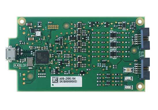
PCBA processing
Why do you choose kingford for PCBA processing?
1. Strength guarantee
▪SMT workshop: We have imported SMT machines and several sets of optical inspection equipment, with a daily output of 4 million. Each process is equipped with QC personnel, who can keep an eye on product quality.
▪DIP production line: We have two wave-soldering machines, among which there are more than 10 old employees who have worked for more than three years. The skilled workers can weld all kinds of plug-in materials.
2. Quality assurance, cost-effective
▪ High-end equipment can stick precision shaped parts, BGA, QFN, 0201 materials. Can also template patch, loose material hand.
▪ Sample and size batch can be produced, proofing from 800 yuan, batch 0.008 yuan/point, no start-up fee.
3. Rich experience in SMT and welding of electronic products, stable delivery
▪ Accumulated SMT SMT processing services for thousands of electronic enterprises, involving many kinds of automotive equipment and industrial control motherboard. The products are often exported to Europe and the United States, and the quality can be affirmed by new and old customers.
▪ On time delivery, normal 3-5 days after complete materials, small batch can also be expedited on the same day shipment.
4. Strong maintenance ability and perfect after-sales service
▪ Experienced maintenance engineers can repair all kinds of patch welding caused by bad products, to ensure the connection rate of each piece of circuit board.
▪ 24-hour customer service staff at any time response, the fastest speed to solve your order problems.

2. Why use multi-layer PCB structure for PCB design?
With the improvement of chip integration, the number of I/O pins in chip package also increases by leaps and bounds, especially with the appearance of BGA package, only by single-sided and double-sided conductor layer wiring can no longer lead out the pin of BGA inner ring.
More importantly, with the development of high-speed signal transmission, high-speed signal wiring needs to use transmission line technology. In high speed PCB design, it is necessary to consider how to optimize the performance of electrical interconnection and control the manufacturing cost of PCB. Reflection, crosstalk, transmission delay and switching noise (SSN) which affect signal integrity are the main problems to be solved in high-speed circuit design.
There are several types of transmission line technology. The earliest was the coaxial transmission line invented by Oliver Heaviside to solve the long-distance transmission problem of telegraphy at the time, while the common forms of transmission line on PCBS are Microstrip and Stripline.
Strip line is a transverse electromagnetic (TEM) transmission line medium invented by Robert M. Barrett in the 1950s, and two years later, a competitor to strip line, microstrip line, was developed by ITT Laboratories.
Microstrip line is located in the outer layer of PCB, the contact with the external environment, so the radiation energy of the microstrip line is easier to radiate to the external environment, and the microstrip line is also susceptible to the influence of the external environment, for example, the welding resistance layer change of εr on the characteristic impedance, so the key high-speed signal is preferred to use the inner line, that is, strip line transmission line.
The multilayer board is also specially equipped with a separate and complete power layer and ground layer, which can not only improve the wiring freedom, but also to prevent signal interference and electromagnetic radiation are favorable, which further promotes the development of PCB multilayer.
Now, with the improvement of IC process technology, digital signal rising edge time is also "passively" shortened. Previously, only need to consider the PCB wire pull through, more and more need to consider the transmission line effect in wiring, so as to better guide electromagnetic wave, avoid signal integrity problems and meet the EMC performance, and single-layer or double-layer board, For the current IC integration and wiring density, it is difficult to have space to construct a good transmission line structure, which requires the use of four layers of board, or even six layers of board, the key signal rich in high harmonics by strip line transmission.
With the development of semiconductor technology, we have to consider using multilayer plate to construct transmission line for electromagnetic wave guidance. For 6-layer boards, there will be BGA or QFN chips. SMT requires the surface smoothness of PCB, and the surface of the sunk metal plate is smooth, which is conducive to welding. It is perfect for high density and high layer board. The disk hole process can also save the surface wiring space occupied by the fan hole and further improve the surface wiring density. In addition, the disk hole process makes the welding pad of the power supply/ground can be directly connected with the main power supply/ground plane through the hole, avoiding the influence of the parasitic inductance of the lead of the fan hole, which is also helpful for the integrity of the power supply.
kingford is a professional PCB design company engaged in electronic products layout layout design, mainly undertake multi-layer, high-density PCB design and circuit board design proofing business, can skillfully use the market mainstream PCB design software, professional and efficient communication to ensure the progress of PCB design, help you to seize the market opportunity earlier!
Which PCB printing method is better?
Feb 24,2023


Just upload Gerber files, BOM files and design files, and the KINGFORD team will provide a complete quotation within 24h.