
Professional PCB manufacturing and assembly
Building 6, Zone 3, Yuekang Road,Bao'an District, Shenzhen, China
+86-13410863085Mon.-Sat.08:00-20:00

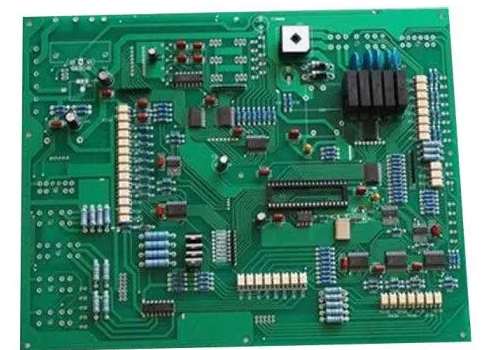
SMT patch refers to the short term for a series of processes based on PCB, Printed Circuit Board (PCB) is printed circuit board. SMT (short for Surface Mounted Technology) is one of the most popular technologies and processes in the electronic assembly industry.
The main characteristics of SMT patch processing
1. High density: Because the number of pins processed by SMT patch is up to hundreds or even thousands, the center distance of pins can be up to 0.3mm, so the high progress BGA on the circuit board needs fine lines and fine spacing. Line widths have been reduced from 0.2~0.3mm to 0.1mm or even 0.05mm, and the double wires between the 2.54mm grids have developed to four, five or even six wires. Thin lines and fine spacing greatly improve the SMT assembly density. In the case of high accuracy of the corresponding SMT patch processing equipment, the corresponding SMT processing plant can be completed.
2. Small aperture: most of the metallized holes in SMT are not used for inserting component pins, and welding is no longer carried out in the metallized holes. The metallized holes only serve as electrical interconnection between layers, so the aperture should be reduced as much as possible to provide more space for SMT patches. The aperture has changed from 0.5mm to 0.2mm, 0.1mm or even 0.05mm.
3, low coefficient of thermal expansion: any material will expand after heating. Polymer materials are usually higher than inorganic materials. When the expansion stress exceeds the bearing limit of the material, the material will be damaged. Due to the large and short pins of SMT, the CTE between the device body and SMT is inconsistent, and device damage caused by thermal stress often occurs. Therefore, the CTE of the SMT board substrate should be as low as possible to accommodate the match with the device.
4, high temperature resistance performance is good: most of today's SMT circuit boards need to install components on both sides. Therefore, SMT processed circuit boards need to be able to withstand two reflow soldering temperatures. At present, lead-free welding is widely used, welding temperature is higher. After welding requirements SMT chip circuit board deformation is small, no bubbling, welding plate still has good weldability, SMT patch circuit board surface still has a high flatness.

Why do you choose kingford for SMT processing?
1. Strength guarantee
▪SMT workshop: We have imported SMT machines and several sets of optical inspection equipment, with a daily output of 4 million. Each process is equipped with QC personnel, who can keep an eye on product quality.
▪DIP production line: We have two wave-soldering machines, among which there are more than 10 old employees who have worked for more than three years. The skilled workers can weld all kinds of plug-in materials.
2. Quality assurance, cost-effective
▪ High-end equipment can stick precision shaped parts, BGA, QFN, 0201 materials. Can also template patch, loose material hand.
▪ Sample and size batch can be produced, proofing from 800 yuan, batch 0.008 yuan/point, no start-up fee.
3. Rich experience in SMT and welding of electronic products, stable delivery
▪ Accumulated SMT SMT processing services for thousands of electronic enterprises, involving many kinds of automotive equipment and industrial control motherboard. The products are often exported to Europe and the United States, and the quality can be affirmed by new and old customers.
▪ On time delivery, normal 3-5 days after complete materials, small batch can also be expedited on the same day shipment.
4. Strong maintenance ability and perfect after-sales service
▪ Experienced maintenance engineers can repair all kinds of patch welding caused by bad products, to ensure the connection rate of each piece of circuit board.
▪ 24-hour customer service staff at any time response, the fastest speed to solve your order problems.
2.PCBA processing manual welding skills
Manual welding is often used in SMT processing factories. In order to make the welding of objects better, we must master the technical essentials of welding. Then how to quickly master the technical essentials of manual welding? Next, Shenzhen PCBA processing manufacturer -kingford to introduce PCBA processing manual welding skills.
PCBA machining manual welding skills
The main tool for manual welding is the electric iron. There are many kinds of electric iron. According to the heating method, it can be divided into direct heat type, induction type, constant temperature electric iron, intelligent electric iron, tin suction pump, hot air welding platform, electric heating clip, etc. Manual welding should first choose anti-static constant temperature electric soldering iron.
1. Welding operation posture
(1) Welding distance
The gas produced in welding will cause harm to the human body, so when using the electric iron, the distance between the nose and the electric iron should be more than 30cm, and 40cm is a more appropriate distance.
(2) electric soldering iron grip method
The electric iron has reverse grip, is holding and holding the pen three grip, the reverse grip is stable, long time operation is not easy to fatigue, suitable for high power electric iron grip, is suitable for medium power electric iron or with elbow electric iron operation, the pen holding method is generally used in welding components and maintenance circuit board.
2. Five-step welding method
(1) Prepare for welding -- clean soldering iron: add tin to the iron head, clean the iron head, which is conducive to heat conduction; Do not use a knife or anything else to scrape the oxide layer of the iron head.
(2) Heating welds: put the soldering iron head on the connection point of the welded metal (the place with the largest heat capacity); Heat begins to flow to the surface of the metal being welded.
(3) solder wetting: the tin wire is placed between the connection point of the soldering iron head and the metal to be welded, forming a thermal bridge; Flux flows in the cold direction, infiltrating the pad -- from the soldering tip to the whole pad, removing the oxide layer and promoting heat conduction; When the solder wire is moved to the opposite side of the heat source, the molten tin flows in the direction of heat, wets the pad and pin, and capillary phenomenon, diffusion, dissolution and metallurgical combination occur at the interface; Push the flux residue toward the surface and edge of the solder joint.
(4) Evacuation of the tin wire: first evacuate the tin wire, after the evacuation of the iron, otherwise the tin wire will solidified on the solder joint.
(5) Stop heating: cooling, solidification, forming solder joints; Note that when the tin wire is not fully solidified, do not shake the components and pcb to avoid virtual welding.
kingfordPCBA processing capability
1. Maximum board card: 310mm*410mm(SMT);
2. Maximum plate thickness: 3mm;
3. Minimum plate thickness: 0.5mm;
4. Minimum Chip parts: 0201 package or parts above 0.6mm*0.3mm;
5. Maximum weight of mounted parts: 150g;
6. Maximum parts height: 25mm;
7. Maximum parts size: 150mm*150mm;
8. Minimum spacing of pin parts: 0.3mm;
9. Minimum ball parts (BGA) spacing: 0.3mm;
10. Minimum ball parts (BGA) ball diameter: 0.3mm;
11. Maximum parts mounting accuracy (100QFP) : 25um@IPC;
12. Patch capacity: 3-4 million points/day.
kingford specializes in providing overall PCBA electronic manufacturing services, including upstream electronic component procurement to PCB production and processing, SMT patches, DIP plug-ins, PCBA testing, finished product assembly and other one-stop services.


Just upload Gerber files, BOM files and design files, and the KINGFORD team will provide a complete quotation within 24h.