
Professional PCB manufacturing and assembly
Building 6, Zone 3, Yuekang Road,Bao'an District, Shenzhen, China
+86-13410863085Mon.-Sat.08:00-20:00

One. Directly or forcibly install the warped PCBA or the warped reinforced frame and install the PCBA in the deformed chassis during the installation of the reinforced frame and the installation of the PCBA and the chassis. Installation stress causes damage and fracture of component leads (especially BGS and other high density IC, surface mounted components), trunk holes of multi-layer PCB, and inner connecting wires and pads of multi-layer PCB
For PCBA or reinforced frame whose warpage degree does not meet the requirements, the designer shall cooperate with the craftsman to take or design effective "cushion" measures at the bow (twist) part before installation.
Tow and analysis
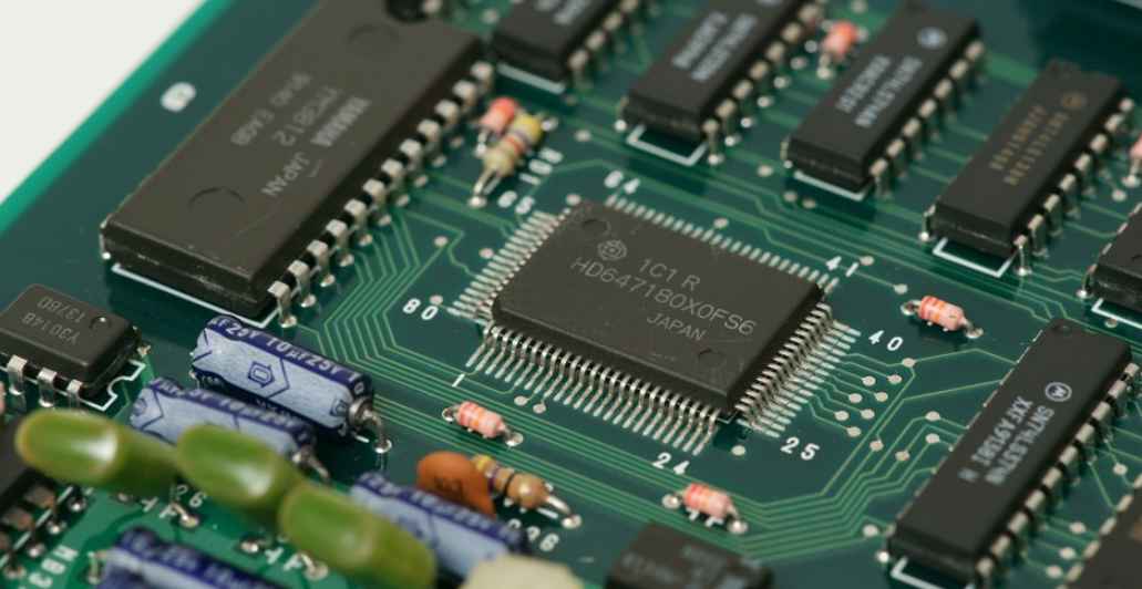
1. Among chip resistance and capacitance components, ceramic chip capacitors have the highest probability of defects, which mainly include the following types:
2. PCBA bow buckling and deformation due to the installation stress of wire bundle.
3. The flatness of PCBA after welding is greater than 0.75%.
4. The design of the two ends of the ceramic disc capacitor is asymmetrical.
5. Common welding pad, welding time is greater than 2s, welding temperature is higher than 245℃, the total number of welding exceeds the specified value 6 times.
6. The thermal expansion coefficient between ceramic chip capacitor and PCB material is different.
7. When PCB is designed, the distance between the fixed hole and the ceramic capacitor is too close, resulting in stress during fastening.
8. Even if the solder pad size of ceramic chip capacitor on PCB is the same, if the amount of solder is too much, it will increase the tensile stress on chip capacitor when PCB board is bent; The correct amount of solder should be 1/2 ~ 2/3 of the solder end height of chip capacitor
9. Any external mechanical or thermal stress will cause cracks in ceramic chip capacitors.
(1) Cracks caused by the extrusion of the mounting pickup head will appear on the surface of the components, usually circular or half-moon cracks with color changes, located in or near the center of the capacitor.
(2) Cracks caused by incorrect setting of the parameters of the placement machine. The picking and placing head of the SMT machine uses a vacuum straw or center clamp to position the component. Excessive Z-axis downward pressure will break the ceramic component. If a sufficient force is applied to a position other than the central area of the porcelain body by the SMT picker, the stress applied to the capacitor may be large enough to damage the component.
(3) Improper selection of the size of the patch pickup head will cause cracks. When the patch picker with small diameter places a concentrated force on the patch, the small ceramic capacitor area will bear greater pressure, leading to cracks in the ceramic capacitor.
(4) Inconsistent solder quantity will produce inconsistent stress distribution on the components, and stress concentration will produce cracks at one end.
(5) The root cause of the crack is the porosity and crack between the layers of the ceramic capacitor and the ceramic plate.
Three. Solution:
Strengthening the screening of ceramic capacitors: The defective ceramic capacitors can be screened by C-SAM and SLAM.


Just upload Gerber files, BOM files and design files, and the KINGFORD team will provide a complete quotation within 24h.