
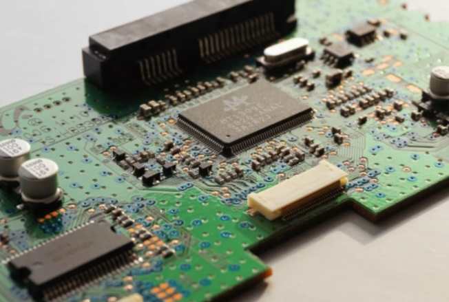
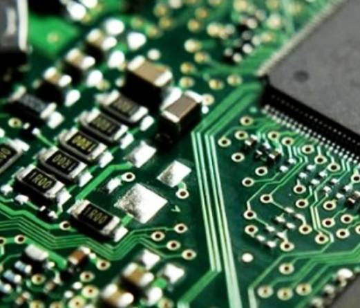
Professional PCB manufacturing and assembly
Building 6, Zone 3, Yuekang Road,Bao'an District, Shenzhen, China
+86-13410863085Mon.-Sat.08:00-20:00

■ SMT mounting process quality inspection, analysis and control
Content: including printing, patch, welding, cleaning and other procedures of the whole process of the quality test methods and strategies, as well as mounting defects analysis and treatment, mounting equipment testing and process parameter control.
■ Traditional quality detection technology and improved quality detection technology
Difference: The "improved quality inspection technique" carries out the corresponding process quality inspection after each critical process.
Within the
■ The main printing quality of solder paste includes
Solder paste, PCB, press, scraper, printing environment, operator, printing parameters, templates, etc
■ Main performance parameters of solder paste
Solder paste viscosity, metal content, melting point, welding temperature, powder size.
Solder paste viscosity: different coating methods choose different viscosity solder paste.
The main factors affecting the viscosity of solder paste are the percentage of metal content of solder paste and the size of solder ball.
■ Metal content of solder paste
Metal composition generally includes: Sn(tin), Pb(lead), Au(gold), Ag(silver), In(indium), Bi(bismuth), Ni(nickel), etc. The main components of solder paste are Sn and Pb.
Lead-free welding paste: Mainly Sn, Ag, Cu(copper).
■ Too low metal content in the solder paste will increase the flux content and reduce the viscosity of the solder paste
Lead to welding spot is not full, resulting in less welding, welding; More holes will appear when welding; Solder joint strength will be greatly reduced;
In the welding will appear more bubbles, easy to cause welding ball and tin beads.
The decrease of metal content leads to the decrease of viscosity, which is prone to collapse and increase the occurrence of bridging.
■ Ideal spherical solder powder requirements
The diameter of the powder should be no more than l / 7 of the template opening size, no more than l / 10 of the nozzle diameter of the applicator.
The solder powder for spherical advantages: than the irregular shape of the solder powder can effectively reduce the particle contact area with the outside, so as to effectively prevent or reduce the oxidation of the solder paste, improve the wettability of welding; Facilitates the rolling effect in the solder paste printing process to fill the template opening.

■ Printing parameters of solder paste
Scraper speed, pressure, Angle, hardness and material, release speed, etc.
Scraper classification: rubber scraper, metal scraper, alloy scraper
Rubber scraper: the hardness is relatively low. There is "digging" phenomenon, easy to wear, rubber scraper hardness: generally (55 ~ 95)Hs,
Metal scraper: Small deformation, little effect on printed solder paste.
Alloy scraper: Alloy scraper with elastic alloy as base and hard metal as blade. Advantages: It has the advantages of both metal scraper and rubber scraper. It has the hardness of metal scraper and the flexibility of rubber scraper. It can print welding paste with flat surface
■ Demoulding speed of solder paste printing
Affect the printed solder paste appearance - printing effect, too long time, easy to residual solder paste at the bottom of the template; Too short time, not conducive to the vertical welding paste, affect its clarity. Pin spacing relation: The smaller the spacing, the smaller the release speed.
Thickness of solder paste
Controlled by the thickness of the template
The relationship between the thickness of the solder paste and the spacing of the pins: (1) The greater the spacing, the greater the thickness of the printing should be. 0.3mm pin spacing -- the template thickness is generally 0.1mm-- the thickness of the printed solder paste is 0.09mm ~ 0.1mm; Devices with 0.5mm or more pin spacing -- template thickness is 0.12mm and 0.15mm-- printing thickness is 0.11mm ~ 0.15mm. The maximum thickness of the template is 0.15mm.
■ AOI technology features (in welding paste quality detection)
■ Solder paste printing defects
Printing offset, insufficient amount of solder paste, excessive amount of solder paste, poor print shape, Smearing/Under Printing, collapse, etc.
■ The main reason for printing deviation: PCB pad and template opening mismatch.
From :www.pcba-smt.cn
■ Insufficient amount of solder paste: the main reason is the size of the template opening.
■ Too much solder paste: the main reason is that the opening is too large.
■ Poor shape of the solder paste: the upper and lower corners of the printed solder paste are extended or appear to collapse, and in serious cases, the leakage and bridge of the solder paste occur. Main reason: solder paste characteristics.
Solder paste collapse can be divided into cold collapse and hot collapse
Cold collapse: after printing, the solder paste slowly spreads to the outside of the pad, from square to arc. From :www.pcba-smt.cn
Reason for cold collapse: low viscosity of solder paste (viscosity is a measure of resistance or resistance to flow)
Solution: Measure the minimum viscosity of the solder paste to prevent collapse and the maximum viscosity of the solder paste to keep rolling in the printing process. The ideal viscosity of the solder paste is between these two values.
Thermal collapse phenomenon: refers to the collapse of well-printed solder paste in the preheating stage of reflow welding.
The reason of heat collapse is related to reflow temperature curve and heating rate.
Solution: Control the temperature rise curve and temperature rise speed.
■ Key factors affecting the quality of the patch: patch force, patch speed/acceleration, patch accuracy, components, solder paste and PCB board. According to the matching principle of the sticker head, the sticker head can be divided into two kinds: no matching claw sticker head and matching claw sticker head.
■ Unmatched middle claw sticker head: Because the sticker head only has a vacuum suction nozzle, so the mechanical damage to the components is small. With a center claw attached to the chip head: the patch head is equipped with a mechanical center claw, which produces a large clamping force on the components, which may cause damage to the components with small size or pins. The patch speed/acceleration affects both the productivity and the quality of the patch. The smaller the component, the higher the accuracy requirements of the patch. A small rotation error or translation error will make the components stick to the offset or even completely deviate from the pad. For a fine-spaced component, a very small rotation error may cause the component to deviate completely, resulting in bridging.
■ Patch accuracy: mainly includes substrate accuracy, substrate positioning accuracy, sticker head positioning accuracy, component positioning accuracy and repeat positioning accuracy of sticker head.
Positioning accuracy: refers to the deviation between the actual placement position and the set position of the placement machine
■ Repeated positioning accuracy: The ability of the mounting head to return to a set point repeatedly.
■ Patch defects: component missing paste, component pasting wrong, component polarity pasting reverse, does not meet the minimum electrical clearance, component pasting bias.
■ Missing component paste: vacuum pickup element is adopted for the suction nozzle of the sticker head.
When the vacuum detector detects a vacuum, it indicates that the component has been picked up. However, if the suction nozzle is blocked by impurities, a vacuum will be formed in the sticker head. At this time, the vacuum detector will also show that the components are picked up, but the components are not actually picked up, resulting in missing stickers.
■ Misplacement of components: The placement machine pastes components to the wrong position. Component mispaste is likely to be the wrong location of the feeder, or when writing the installation program to fill in the wrong component data, or program Settings and the feeder does not match.
■ IPC standards classify electronic products
There are three levels: Level 1, Level 2, and Level 3. The higher the level, the higher the performance requirements and the stricter the acceptance conditions.
(1) Level 1: General electronic products (civil)
(2) Level 2: Special service electronic products (industrial and commercial)
(3) Level 3: high-performance electronic products (medical, military, aerospace)
■ Four quality acceptance conditions of all levels of products stipulated in IPC standards: target conditions, acceptable conditions, defect conditions, process warning conditions.
Target condition (also known as "ideal" condition) : An ideal condition that is close to perfection.
Acceptable condition (also known as "acceptable" condition) : It means that the component can guarantee complete and reliable operation under the use environment (but not as perfect as the target condition). It is a necessary quality acceptance condition to ensure the quality of products.
Defect condition (also known as "reject" condition) : refers to the component's integrity, installation or function cannot meet the requirements under the use environment, the defect condition should be rejected or unqualified for the product. Such products should be reworked, repaired, scrapped or "disposed of by the book".
Process warning condition (also known as "qualified for Improvement" condition) : refers to a condition that does not affect the integrity, installation and function of the product, but does not meet the required conditions (non-rejection).
IPC-A-610D: Unless it is determined to affect the integrity, installation, and function of the product as specified by the end User, circumstances not covered by the rejection conditions and process Warning conditions are considered acceptable.
Electronic products that are "defect conditions" and "process warning conditions" should generally be rejected.
However, as long as they have been reworked, repaired or "treated by the rules", or have been effectively and continuously improved, these products may become "improved" (or degraded) products that meet the requirements in their integrity, installation or function under the circumstances of use, and shall be accepted as meeting the minimum requirements of the final product and shall not be included in the rejection.
Electronic mounting welding quality inspection method: visual inspection, automatic inspection commonly used solder joint quality automatic inspection: automatic optical inspection (AOI) and automatic X-ray inspection (AXI)
■ Solder joint detection has the following two principles:
① The principle of full inspection: the use of visual or instrument inspection, inspection rate should reach l00 %
(2) Non-destructive principle: In addition to spot inspection of solder joints, it is not recommended to use inspection and evaluation methods that are easy to damage solder joints, in order to reduce the detection cost.
■ AOI detection component: AOI is composed of optical part and image processing part.
Optical part function: To obtain the image of the solder joint to be detected. The optical part includes CCD camera, lens, light source (mostly LED light source), acquisition card and movement platform, to analyze, process and judge whether there are various welding defects.
Compared with AOI, the biggest advantage of AXl is that it can detect the inherent defects of solder joints and hide solder joints by BGA and other devices.
■ Common wave soldering process problems are: non-wetting/semi-wetting, tin ball, disturbed solder joint, cold welding, tip, bridge, virtual welding.
■ Reflow welding defects are mainly divided into two categories: one is related to metallurgical phenomena, including cold welding, semi-wetting, non-wetting, excessive intermetallic compounds; The other is related to the abnormal solder joint, including insufficient solder, bridge, tin ball, tin bead, offset, core suction, cavity, monument, etc.
■ Lead-free welding defects: tin crack, solder joint stripping, "Black Pad" (Black Pad), cavity greatly increased
Cleaning quality: After PCB welding, a variety of residues remain. The most typical and main residues are white spots and carbonized residues, which mainly come from flux.
■ Main components of white spot: flux residues or other materials react with flux. White spot reduction method: The key is to control the flux
■ Carbonization residue caused by overheating, carbonization means overheating and oxidation, the thinner the flux film, the easier to produce overheating and oxidation. Solution: From the source of "overheating", there are two ways to solve the problem: one is to avoid overheating; The other is to make the relevant materials (mainly flux and welding resistance film) can resist heat.
■ PCBA cleaning quality test method
1. Test methods for ionic pollutants: (1) extraction solution resistivity test method, (2) ion chromatography test method
2. Flux residue test method
3. Surface insulation resistance test method


Just upload Gerber files, BOM files and design files, and the KINGFORD team will provide a complete quotation within 24h.