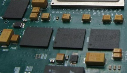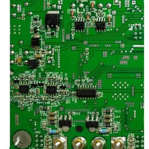
Laser technology is playing an increasingly important role in the field of 3C electronics, involving cutting, welding, punching and other processes. With the gradual development of electronic products to fine and intelligent, more materials are applied in them. A full understanding of the characteristics of various materials used in electronic products will be conducive to the use of more suitable laser processing technology and flow.
The ideal electronic packaging substrate material must meet the following basic requirements:
(1) High thermal conductivity, low dielectric constant, good heat resistance and pressure resistance;
(2) The thermal expansion coefficient is close to the chip material Si or GaAs to avoid the thermal stress damage of the chip;
(3) It has enough strength and stiffness to support and protect chips and electronic components;
(4) The cost should be as low as possible to meet the needs of large-scale industrial production and application;
(5) Good processing, assembly and installation performance. The commonly used electronic packaging substrate materials include organic packaging substrate metal composite substrate and ceramic packaging substrate three categories.
Compared with traditional substrate materials, ceramic substrate has many advantages:
(1) High thermal conductivity, heat generated by high integration package can be discharged in time;
(2) Strong chemical stability, in the process of processing can resist acid, alkali, organic solvent corrosion, does not produce discoloration, swelling and other characteristics change;
(3) Good insulation performance and high reliability
(4) Small dielectric coefficient, good high-frequency characteristics, can reduce the signal delay time;
(5) High mechanical strength, good dimensional stability, so that the components installation accuracy is high;
(6) Strong heat resistance, inorganic substrate material glass transition temperature is generally higher than organic substrate material, in the process of thermal shock and thermal cycle is not easy to damage;
(7) The thermal expansion coefficient of inorganic substrate materials (2.3-10 ppm/℃) is generally lower than that of organic substrate materials (higher than 12 ppm/℃).

Therefore, ceramic materials gradually developed into the new generation of integrated circuit and power electronic module of the ideal packaging substrate, ceramic circuit board packaging technology has been widely concerned and rapid development. Table 1 shows the performance comparison between commonly used ceramic packaging materials and Si. Currently, commonly used ceramic substrate materials include Al2O3, SiC, BeO and AlN.
Common ceramic metallization techniques include: thin film process, thick film process, direct copper coating and laser activated metallization.
1 Thin film method
As a wafer level manufacturing technology, thin film process is the main method of metal film deposition in microelectronics manufacturing. FIG. 1 shows the process flow of ceramic circuit board prepared by thin film technology. First, a 200-500 nm Cu layer is deposited on the ceramic surface by surface deposition processes such as evaporation and magnetron sputtering, so as to facilitate the subsequent plating process. Then, through the film, exposure, development and other processes to complete the pattern transfer, then electroplating to increase the Cu layer to the required thickness, and finally through the film removal, etching process to complete the production of conductive lines.
In recent years, ceramic circuit boards prepared by thin-film technology have shown strong competitiveness in power type LED packaging. However, there are still many problems in the thin film process, including the unstable binding force between the metal layer and the substrate. Before the deposition of Cu layer, a layer of Ti should be deposited as a transition layer to enhance the binding force between the Cu layer and the ceramic. After the completion of the pattern transfer, Ti needs to be etched, which increases the complexity of the process. When making double-sided circuit boards, it is difficult for the deposited seed layer to enter the micropore, and there is no Cu in the pore wall. In addition, thin-film technology requires expensive manufacturing equipment, high vacuum conditions and low production efficiency.
2. Thick film method
Thick film method is a method of directly depositing conductive paste on substrate through micro-flow direct writing technology such as screen printing technology, micro straight writing technology and inkjet printing technology, and sintering at high temperature to form conductive lines and electrodes. This method is suitable for most ceramic substrates. Figure 3 shows the process flow of making ceramic circuit board by thick film technology. Thick film conductive paste is usually composed of metal powder with the size of micron or even nano level and a small amount of glass binder plus organic solvent. The glass binder in the slurry is combined with the substrate at high temperature to make the conductive phase adhere to the surface of the substrate and form a conductive circuit.
Thick film method with screen printing technology is the most widely used, the technology has the advantages of simple process, but the disadvantages are also obvious: limited by the size of conductive paste and screen, the minimum wire width of the prepared wire is difficult to be less than 60µm, and can not make three-dimensional graphics, so it is not suitable for small batch, fine circuit board production. Although micro-straight writing technology and inkjet printing technology can deposit high-precision conductive graphics, they require high viscosity of slurry and are prone to channel blockage. In addition, the conductive circuit formed by the thick film method has poor electrical performance and can only be used in electronic devices with low power and size requirements.
3. Direct copper application method
Direct Bonded Copper (DBC) technology is a ceramic surface metallization technology mainly developed based on Al2O3 ceramic substrate, and later applied to AlN ceramics, which has been widely used in automotive, electric power, aviation, aerospace and military and other fields.
Pure copper does not wet the Al2O3 ceramic in the molten state, so oxygen element needs to be introduced into the reaction interface. The Cu-Cu2O eutectic liquid produced at high temperature has good wettability for Al2O3. The copper foil can be directly deposited on the Al2O3 ceramic substrate by using the CuAlO2 generated as the transition layer. In general, oxygen is introduced in the following two ways:
(1) The copper foil is pre-oxidized in the air to produce CuO of a certain thickness;
(2) Copper foil is weakly oxidized in nitrogen to produce Cu2O with a certain thickness. Both work in much the same way, with the first method being more practical.
The main disadvantages of DBC technology are that the thickness of copper foil is large, it is difficult to obtain high-precision wire through the subsequent chemical etching process, and the interface oxygen element is difficult to control, and the porosity between copper foil and ceramics is easy to occur, resulting in the final device performance is unstable, which remains to be further studied in basic technology. In addition, due to the limitation of technical principles, copper foil coating can not achieve through hole metallization.
4. Laser activated metallization
Laser activated metallization is a two - step process. The specific method is to combine the laser direct writing process and the traditional electroless plating process, so as to further improve the forming efficiency and reduce the production cost. By combining laser direct writing process with electroless plating process, conductive circuit can be formed directly on the surface of non-metallic substrate. First, metal compounds are induced by laser direct writing technology to decompose and deposit on the substrate surface, "implanted" metal particles on the substrate surface to form a "catalytic" center for subsequent electroless plating. In fact, this step not only implants the "catalytic" center, but also enables the graphic of the board. Secondly, electroless plating process does not require external current. Metal salts and reducing agents in the chemical plating solution are used for REDOX reaction on the surface of the substrate material with catalytic activity to produce metal deposition. Electroless plating technology has become a main process for manufacturing integrated circuits and microdevices because of its simple equipment, low pollution to the environment and low cost. Because only the laser activated region has catalytic activity, the laser activated metallization technology can form high-precision and high-purity metal patterns on the surface of ceramic board.


