
Professional PCB manufacturing and assembly
Building 6, Zone 3, Yuekang Road,Bao'an District, Shenzhen, China
+86-13410863085Mon.-Sat.08:00-20:00

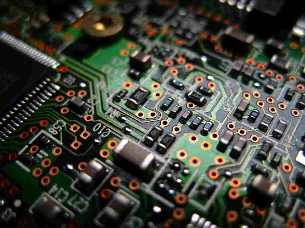
PCB Layout Guide will mention the corner Angle problem of high-speed signal routing. It will say that high-speed signal should be routed at a 45 degree Angle rather than a right Angle, and it will say that circular arc is better than a 45 degree corner.
Is this the case? How to set the PCB line Angle, is it better to walk 45 degrees or walk the arc? Is it okay to walk at a 90 degree Angle?
1. Can PCB be routed at an acute Angle?
Can PCB line at an acute Angle, the answer is no, regardless of whether the acute Angle line will cause negative impact on high-speed signal transmission lines, from the PCB DFM aspect alone, should avoid the occurrence of acute Angle line.
Because the PCB wire intersects at an acute Angle, it will cause a problem called acid Angle "acid traps", in the PCB board process, in the PCB circuit etching link, at the "acid traps" will cause excessive corrosion of PCB circuit, resulting in the problem of PCB circuit breakdown.
While DFF Audit with CAM 350 can automatically detect potential problems with acid traps to avoid bottlenecks when PCBS are being manufactured, if PCB factory technicians detect acid traps, they will simply place a piece of copper into the gap.
In fact, engineers in many board factories do not know layout. They just repair acid trap from the perspective of PCB engineering processing. However, it is not clear whether such repair will bring further signal integrity problems. Therefore, we should try to avoid acid trap from the source in layout.
How to avoid sharp Angle when pulling cable, resulting in acid trap DFM problem? Modern EDA design software (such as Cadence Allegro, Altium Designer, etc.) is equipped with perfect Layout routing options. We use these auxiliary options flexibly in layout routing. It can greatly avoid the "acid trap" phenomenon when we produce layout
The outlet Angle of the welding pad is set to avoid the Angle between the wire and the welding pad forming an acute Angle.
Using the Enhanced Pad Entry function of Cadence Allegro, we can avoid as much as possible the Angle between wire and pad when exiting the wire in layout, and avoid the problem of "acid traps" DFM.
Flexible application of Cadence Allegro to switch the "toggle" option when wiring can avoid the formation of acute Angle Angle when the wire pulls out the T-branch and avoid the problem of "acid traps" DFM.
2. Can PCB layout be routed at 90°
High frequency and high speed signal transmission line should avoid the 90° corner line, is a variety of PCB Design Guide to strongly request, because high frequency and high speed signal transmission line needs to maintain the characteristic impedance is consistent, and the 90° corner line, at the corner of the transmission line, will change the line width, 90° corner line width is about 1.414 times of the normal line width, As the linewidth changes, the signal will be reflected, and the extra parasitic capacitance around the corner will also delay the transmission of the signal.
Of course, when the signal is propagated along the uniform interconnect, there will be no reflection and distortion of the transmitted signal. If there is a 90° corner on the uniform interconnect, there will be a change in the width of the PCB transmission line at the corner. According to the calculation of relevant electromagnetic theory, this will definitely bring the reflection effect of the signal.
In theory, but theory is theory. In practice, does a 90-degree corner have a significant impact on high-speed signal lines?
90° corners have a negative effect on high-speed signal lines, theoretically, but are they fatal? Does the 90° corner have the same effect on high speed digital signal and high frequency microwave signal transmission lines?
According to this paper "right angle corners on printed circuit board traces,time and frequency domain analysis" and Howard Johnson "Who's Afraid of the Big Bad Bend? And Eric Bogatin's book Signal Integrity and Power Integrity Analysis (Second Edition), Chapter 8, we can draw the following conclusions:
For high-speed digital signals, a 90° corner will have a certain impact on high-speed signal transmission lines. For high-density high-speed PCB, the width of the wire is generally 4-5mil, and the capacitance of a 90° corner is about 10fF. It is estimated that the cumulative delay caused by this capacitance is about 0.25ps. A 90° corner on a 5mil wire width wire would not have much impact on today's high speed digital signal (100-psec rise edge time).
For high-frequency signal transmission lines, in order to avoid signal damage caused by Skin effect, a wider signal transmission line is usually used, such as 50Ω impedance and 100mil line width. The line width at the 90° corner is about 141mil, and the signal delay caused by parasitic capacitance is about 25ps. A 90° corner will have a serious impact.
At the same time, microwave transmission lines always hope to minimize the signal loss, impedance discontinuity at 90° corner and outside the parasitic capacitance will cause high-frequency signal phase and amplitude errors, input and output mismatch, as well as the possible existence of parasitic coupling, and then lead to the deterioration of circuit performance, affecting the transmission characteristics of PCB circuit signals.
The influence of a single 90° corner on the signal quality of the high-speed digital transmission line, relative to the deviation of the height of the wire and the reference plane, the change of line width and line distance uniformity in the etching process of the wire itself, the change of the dielectric constant of the plate on the frequency signal, and even the influence of the parasitic parameters of the hole are much greater than the problems brought by the 90° corner.
But today's high-speed digital circuit transmission line always can't avoid winding equal length, a dozen or twenty corners stack up, the cumulative effect of the 90° corner stack up caused by the signal rise delay will become not negligible. High-speed signals are always transmitted along the path of impedance, around the 90° corner of the same length, the final actual signal transmission path is slightly shorter than the original.
And now the high-speed digital signal transmission rate is becoming higher and higher, the current HDMI2.0 standard, the transmission bandwidth rate has reached 18Gbps, 90° corner line will no longer meet the requirements, now EDA software even those who use, for 45° line has been supported very well.
At the same time, 90° corner line, in terms of engineering aesthetics, is not in line with people's aesthetic. Therefore, for the current layout, no matter whether you take the high frequency/high speed signal line, we should try to avoid the 90° corner of the line, unless there are special requirements.
For high-current wiring, sometimes we will replace the wiring with copper skin. At the corner of copper laying, it is also necessary to replace the 90° corner with two 45° corners, which is not only beautiful, but also does not have EMI hidden trouble.
3. Route at 45°
In addition to RF signals and other signals with special requirements, the wiring on our PCB circuit board should preferably be routed at 45°. It should be noted that when 45° Angle is used to wrap around the same length, the length of the corner should be at least 1.5 times the width of the line, and the spacing between the lines should be at least 4 times the width of the line.
Because high-speed signal lines are always transmitted along the path of impedance, if the spacing around the isometric lines is too close, the high-speed signal takes a shortcut due to the parasitic capacitance between the lines, and the isometric error will occur. Modern EDA software winding rules can be very convenient to set the relevant winding rules.
4. Route with arc arc
If it is not clearly required by the technical specification to use arc line, or rf microwave transmission line, I think it is not necessary to use arc line, because of the layout of high-speed high-density PCB, a large number of arc line in the later repair is very troublesome, and a large number of arc line is relatively expensive space.
For high-speed differential signals like USB3.1 or HDMI2.0, I think it is still possible to go down the arc line and install bi.
Of course, for RF microwave signal transmission line, or priority to walk the arc line, or even to walk the "45° external miter" line
5. Line at any Angle
With the development of 4G/5G wireless communication technology and the continuous upgrading of electronic products, the transmission rate of PCB data interface has reached more than 10Gbps or 25Gbps at present, and the signal transmission rate is still developing towards high speed. With the development of high speed and high frequency signal transmission, higher requirements are put forward for PCB impedance control and signal integrity.
For digital signals transmitted on PCB board, many dielectric materials used in the electronics industry, including FR4, have been considered uniform at low and low frequency transmission.
However, when the electronic signal rate on the system bus reaches Gbps level, this assumption of uniformity is no longer valid. At this time, the local changes in the relative dielectric constant of the dielectric layer caused by the gaps between the glass fiber bundles interwoven in the epoxy resin substrate will not be ignored. The local perturbation of the dielectric constant will make the delay and characteristic impedance of the line spatially correlated, thus affecting the transmission of high-speed signals.
The test data based on the FR4 test substrate show that due to the relative position difference between the microstrip line and the glass fiber bundle, the effective dielectric constant of the measured transmission line fluctuates greatly. Although these spatial perturbations appear to be small, they will seriously affect the differential transmission line with data speed of 5-10Gbps.


Just upload Gerber files, BOM files and design files, and the KINGFORD team will provide a complete quotation within 24h.