
Professional PCB manufacturing and assembly
Building 6, Zone 3, Yuekang Road,Bao'an District, Shenzhen, China
+86-13410863085Mon.-Sat.08:00-20:00

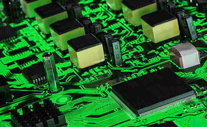
Bluetooth circuit Board Design Guide
Printed circuit boards using Bluetooth technology may experience interference, data loss, and poor signal integrity if certain precautions are not taken. We will outline many of the rules and guidelines to consider when choosing Bluetooth technology for a specific application, especially when designing it onto a circuit board.
A variety of applications utilize Bluetooth, including:
l Beacons used in shopping malls
l Eddy current frames for industrial sensing applications
l Headphones and audio/stereo products
l Remote peripherals, such as video game controllers or computer mice/keyboards
l Home automation system
l Wireless consumer electronics applications, including cameras, printers and phones
Each application uses the same generic Bluetooth technology, but uses it differently, and depending on the type of connection, design engineers need to combine fundamentals to optimize signal integrity and overall device efficiency.
Huachu DFM

Bluetooth isn't a very fast wireless option compared to Wi-Fi, but it's getting faster and faster. It also doesn't penetrate walls and other nearby obstacles very well, and has poor range.
While still a work in progress, it's still a good choice (5.0 is the latest update and a nice improvement over 4.2). In most cases, it is a low power, reliable, secure, and widely supported option that can be easily implemented on a variety of small peripherals.
Bluetooth technology is over 20 years old and still evolving, and although Bluetooth technology has improved over the years in terms of speed, power, range, security and other attributes, it still seems to suffer from some of the same issues since the concept was first introduced in the mid 90s, including its sensitivity to signal interference.
So, from a PCB design perspective, what can be done to optimize signal integrity and minimize interference and lost packets?
Here are some Bluetooth circuit design considerations and general rules of thumb:
Use authenticated modules
1. If Bluetooth is integrated into a product and resources are limited, consider using pre-certified, fully included modules to help speed development and time-to-market. It may end up costing a little more, but it usually avoids some of the hassle caused by antenna placement/design and EMI sensitivity.
There are several reasonably priced certified modules on the market today, most of which incorporate small ARM processors, such as Microchip's RN4020 or RN4870 or Silicon Labs' BT121 or BGM113. Having the processor mounted on the board gives it greater flexibility and functionality, for example, in addition to its Bluetooth stack, simple peripherals can be controlled via GPIO, SPI, I2C, PWM, etc.
Check your Bluetooth device selection
2. Make sure you choose the right Bluetooth device for the application and that the antenna is the right size and adjustment.
If you are using a simple beacon application that requires only short bursts/intervals to announce location or data, low power (Bluetooth low power or BLE), cost-effective solutions with minimal features and peripherals can be used to save on-board real estate and final costs.
If you are looking for more products for higher throughput, audio streaming, or data exchange Bluetooth applications, then you may want products with higher transmit power, higher receive sensitivity, and faster data rates (albeit at reduced data transfer speeds) that generally help minimize packet loss.
If you are looking for a multi-in-one chip, consider using a chip set that contains powerful or auxiliary processors including available UART, SPI, I2C, PWM, ADC, DAC, and GPIO pins.
If you are working with content that relies heavily on RSSI readings, make sure that its RSSI monitor has adequate dB resolution.
Separation or removal of copper signals and high-energy components
3. When designing in a Bluetooth chip set or module, keep the antenna area completely away from nearby copper signals or components carrying large amounts of energy (especially power paths switched by boost or step-down converters).
This also includes making areas (and laminates) free of planes and polygons. Most Bluetooth chipset manufacturers will provide layout guidelines that should be followed strictly during PCB design. If you are laying out the antenna area manually, use the ground plane appropriately to maintain good bandwidth at the input and be sure to leave enough room for the tuned elements (printed and ceramic antennas require ground planes).
Use ground wire trace through holes to prevent unwanted radiation from the PCB edge, as it may penetrate nearby Bluetooth signals. If you can, try optimizing the shape of the board for the location of the Bluetooth device and its antenna by placing it on the edge and away from nearby components and signals. If using analog based signals such as audio, make sure that analog and digital connections are separated.
It is always a good idea to shield electronics (not antennas, of course) to prevent cross-coupling and minimize noise.
Power supply precautions
4. Ensure that the rails powering the Bluetooth module or chip are clean, and use bypass (1.0uF) and decoupling capacitors (0.1uF and 10nF) when needed. Ferrite magnetic beads can also be used on the power rail to enter the Bluetooth area of the board to suppress high-frequency noise.
Tools and analysis
5. If designing the antenna area, make sure you have the appropriate equipment (such as a network analyzer) to analyze and tune the matching network, or consider sending the design to a third party RF test lab.
Consider real-world obstacles
6. There are many things that can cause blocking or distuning during a Bluetooth connection, including nearby water (and humans... We are mainly water), metallized objects, smartphones/tablets, computers, operating devices on the same ISM band, such as microwave ovens or WLAN technology, power supplies, wireless RF video, office lighting and home phones.
Even when paired at close distances (1-2 meters), it is highly susceptible to signal loss. If such conditions have a higher risk of affecting signal quality, choose a device with higher power and run at a lower speed to minimize packet loss. Alternatively, if the electronics are located inside the housing, make sure that the metallized material is minimized and kept away from the BLE module. The relationship between Bluetooth signal strength and distance is not linear. In fact, it's very non-linear, somewhat unpredictable depending on the environment, but it does follow a general pattern.
Whether you are designing a small, simple Beacon module or a data-streaming, power-hungry Bluetooth hub, following these considerations can save you a lot of trouble during the test/implementation phase of your design.
With the expansion of Bluetooth PCB components, now is an exciting time to integrate wireless communication and control into products, and the future will only bring smaller, faster, cheaper and more powerful Bluetooth components.
Printed circuit board assembly technology
Feb 12,2023


Just upload Gerber files, BOM files and design files, and the KINGFORD team will provide a complete quotation within 24h.