
Professional PCB manufacturing and assembly
Building 6, Zone 3, Yuekang Road,Bao'an District, Shenzhen, China
+86-13410863085Mon.-Sat.08:00-20:00

The guarantee quality of four-layer circuit board is defined in IPC, the appearance process is anti-oxygen, the vacuum packaging is not removed, it will be used within half a year, the vacuum packaging is removed within 24 hours, and it is under the background that the temperature and humidity degree is controlled, the board will be used within the next year in the undismantled packaging, the internal solution should be finished within a week, the temperature and humidity degree should also be controlled. Gold plate is equivalent to tin plate, but the choke process is stricter than tin plate.
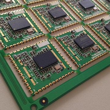
Generally speaking, the four-layer circuit board can be divided into the top layer, the bottom layer and two mid-waist layer.
Four-layer circuit board refers to that the line printing board is made of 4-layer glass fiber. Generally, four-layer circuit board will be used in SDRAM, which will increase the cost of PCB but can avoid the disturbance of noise.
Common Rules for Layering and Routing multilayer PCB Circuit boards Common rules for layering PCB circuit boards are as follows:
(1) The setting principle of the spacing of the printed wiring of the component. The spacing constraint between different networks is set by the spacing of printed wiring of electrical insulation, manufacturing process and components. Volume and other factors vote. For example, if the Clearance Constraint of a chip component is 8mil, the clearance constraint cannot be set to 10mil. The PCB board presets a 6mil PCB presets rule for the chip. At the same time, the setting of spacing should also consider the problem to the labor capacity of the manufacturer.
In addition, one of the factors affecting the element is the electrical insulation, if the potential difference between the two components or the network is large, the need to consider the problem of electrical insulation. The voids in a normal background are 200V/mm below volt, which is 5.08V/mil. Therefore, when there are both high-voltage and low-voltage circuits on the same circuit board, adequate safety spacing is required. When there is a high voltage circuit and a low voltage circuit, it is necessary to add sufficient safety spacing.
(2) The selection of corner routing mode. In order to make the circuit board easy to make a harmonious view, the PCB circuit board preset needs to set the standard style of the line corner, the selection of the line corner way. You can choose 45°, 90° and arc. Generally do not think it is appropriate to use a sharp corner, it is better to think it is appropriate to use an arc transition or 45° transition, prevent think it is appropriate to use 90° or more sharp corner transition.
The joint sign between the wire and the pad should also try to be sophisticated, to prevent the exposure of small pointed feet, can be considered appropriate and use the way to solve the tear drop. When the core distance between pads is less than the outer diameter D of a pad, the width of the wire can be the same as the diameter of the pad; If the core distance between the pads is greater than D, the width of the wire is not suitable for greater than the diameter of the pads. The time when a conductor passes between two pads without communication with them, shall maintain the maximum and equivalent spacing with them. The time when a conductor and a conductor of a conductor passes between two pads without communication with them, shall maintain the maximum and equivalent spacing with them, and the spacing between them shall also be equal and maintain the maximum. The spacing between them should also be equal on average and maintained at maximum.
(3) the printed width of the line is confirmed. The width of the wire is determined by the current level of the wire and anti-interference factors. The larger the current through the current, the wider the wire should be. The power cable should be wider than the signal cable. In order to ensure the stability of the ground potential (the larger the volume of the ground current conversion, the wider the line should be. The ordinary power line should be wider than the signal line, the power line should be wider than the signal line, the impact should be less), the ground wire should be wider, the ground wire should be wider. Empirical verification: When the thickness of the copper film of the printed wire is 0.05mm, the flow-carrying ground wire of the printed wire should also be wide. The calculation can be carried out according to 20A/mm2, that is, the wire of 0.05mm thick and 1mm wide can flow through the current of 1A. So for the ordinary for the ordinary width can be satisfied with the requirements; High voltage High voltage, signal line 10 ~ 30mil width can be satisfied with the requirements of high voltage, large current signal line width is equal to 40mil, line to line spacing is greater than 30mil. In order to ensure the anti-shedding strength and office reliability of the wire, in the plate plane or the size and density of the surface of the object permitted range, should consider appropriate and use as wide as possible wire to reduce the line impedance, increase anti-interference performance.
For the width of the power line and ground wire, in order to ensure the stability of the waveform, in the case of the circuit board wiring space permitted, try to bold, ordinary things at least 50mil requirements.
(4) Anti-interference and electromagnetic shielding of printed wire. The interference on the wire mainly includes the interference introduced between the wires, the interference introduced by the power line) printed wire anti-interference and electromagnetic shielding. The interference on the wire mainly includes the interference introduced between the wires, and the crosstalk between the signal lines, and the crosstalk between the signal lines, etc., reasonable placement and placement of wiring and grounding form can reduce the interference source, so that the PCB circuit board preset circuit board has better electromagnetic compatibility performance.
For high frequency or other tightly closed signal lines, such as the clock signal line, on the one hand, the line should be as wide as possible. For high frequency or other tightly closed signal lines, such as the clock signal line, on the one hand, the line should be as wide as possible. On the other hand, the signal line can be wrapped with a closed ground wire. "Wrap" is equivalent to adding a package of ground to isolate it from the surrounding signal line is to use a closed ground wire to "wrap" the signal line, grounding shield layer). Layer grounding shield).
For analog and digital to separate wiring, can not be mixed. For analog and digital to separate wiring, can not be mixed. If the demand will eventually unify analog and digital ground into a potential, it should generally be considered appropriate to use a bit of ground, that is, only select a bit will analog and digital ground together, to avoid forming ground loop, resulting in ground potential offset.
After the completion of wiring, should be in the top and bottom without repair wire place to apply the large plane or object surface size of the ground copper film, also known as copper, to reduce the completion of wiring, should be in the top and bottom without repair wire place to apply the large plane or object surface size of the ground copper film, also known as copper, to reduce the ground impedance of the pipe, Thus, weakening the high frequency signal in the ground wire and grounding the size of the large plane or object surface can act as a restraining effect on electromagnetic interference. Small ground impedance, thus weakening the high frequency signal in the ground, while large plane or object surface size ground can be a limiting effect on electromagnetic interference. A parasitic capacitance that can restrict electromagnetic interference due to the ground size of a large plane or object surface, and is particularly harmful for high speed circuits; At the same time, one hole in a circuit board with too many holes can introduce about 10pF of parasitic capacitance, which is particularly harmful for high-speed circuits and reduces the mechanical strength of the circuit board. Therefore, when wiring, it should be possible to reduce the number of holes. In addition, in the use of perforated holes in the wiring, it should be possible to reduce the number of holes in the wiring (through the hole), the general use of pad to replace. This is because when the circuit board is manufactured, it may be due to the end of the processing caused by some perforating holes (through holes) have not been pierced, and the welding pad can certainly be pierced when processing, which is equivalent to the convenience of manufacturing.
The above is the general principle of PCB layout and wiring, but in practice, the layout and wiring of components is still a very flexible office, the layout of components and the form of wire is not unique, the final result of layout and wiring is still very much determined by the PCB circuit board as a position of the experience and thinking of the clues. It can be said that there is no standard can determine the outcome of the layout and wiring scheme is right and wrong, can only compare the relative good and bad. Therefore, the above layout and wiring principles only as the PCB circuit board preset reference, practice is the only standard to determine the pros and cons of the outcome.


Just upload Gerber files, BOM files and design files, and the KINGFORD team will provide a complete quotation within 24h.