
Professional PCB manufacturing and assembly
Building 6, Zone 3, Yuekang Road,Bao'an District, Shenzhen, China
+86-13410863085Mon.-Sat.08:00-20:00

1, the width of the circuit board is ≤260mm (SIEMENS line) or ≤300mm (FUJI line); If automatic dispensing is required, width × length of PCB assembly board is less than 125mm×180mm.
2, the appearance of the board as close to the square as possible, recommended to use 2×2, 3×3...... A Mosaic board; But not a yin-yang board.
3. The outer frame of the circuit board (clamping edge) should adopt a closed-loop design to ensure that the PCB board will not be deformed after it is fixed on the fixture.
4, the center distance between the small board is controlled between 75mm ~ 145mm. Wechat official account: Shenzhen LED Chamber of Commerce
5, the connection point between the outer frame and the inner small board, small board and small board shall not have large devices or protruding devices, and the edge of the components and PCB circuit board shall be left more than 0.5mm space, to ensure the normal operation of the cutting tool.
6, open four positioning holes at the four corners of the outer frame of the plate, the aperture of 4mm±0.01mm; The strength of the hole should be moderate to ensure that it will not break in the process of upper and lower plate; Aperture and position accuracy should be high, hole wall smooth without burr.
7, each small board in the circuit board should have at least three positioning holes, 3mm≤ aperture ≤6mm, edge positioning holes within 1mm is not allowed to wire or patch.
8. Reference symbol for the positioning of the whole board of the circuit board and for the positioning of the fine-spaced device. In principle, QFP with spacing less than 0.65mm should be set in its diagonal position; The positioning reference symbols for the PCB should be used in pairs and arranged diagonally on the positioning elements.
9. When setting the reference anchor point, an open weld area 1.5mm larger is usually left around the anchor point
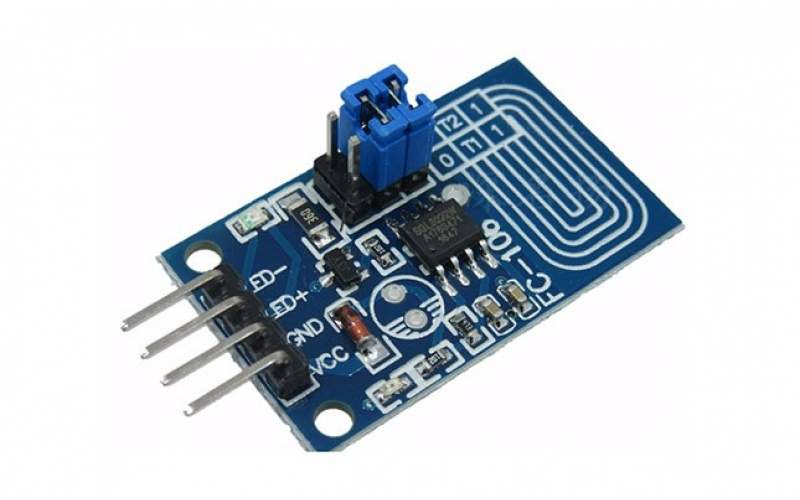
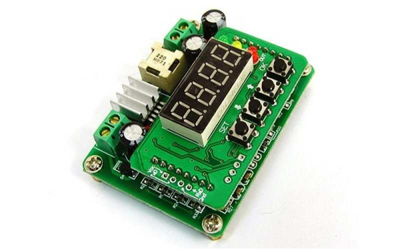
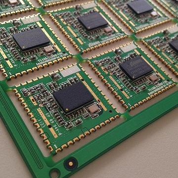
PCB circuit board appearance
Bare Board (a board with no parts attached) is also often referred to as the "Printed Wiring Board (PWB)". The substrate of the board itself is made of an insulating, non-bendable material. The small wire material that can be seen on the surface is copper foil. Originally, copper foil is covered on the whole board, but in the manufacturing process, the middle part is etched away, and the remaining part becomes a network of small lines. These circuits are called conductor patterns, or wiring, and are used to provide circuit connections for parts on the PCB.
Usually the PCB is green or brown in color, which is the color of solder mask. It is an insulating protective layer, which can protect copper wire, prevent short circuit caused by wave soldering, and save the amount of solder. A silk screen is also printed on top of the solder shield. It is usually printed with words and symbols (mostly white) to indicate the position of the parts on the board. Screen printing is also known as legend.
In the final product, integrated circuits, transistors, diodes, passive components (such as resistors, capacitors, connectors, etc.) and a variety of other electronic components are installed. Through wire connection, can form electronic signal connection and function.
PCB circuit board main advantages
The main advantages of using printed boards are:
1. Due to the repeatability (reproducibility) and consistency of graphics, wiring and assembly errors are reduced, saving the maintenance, debugging and inspection time of equipment;
2, the design can be standardized, conducive to interchange;
3, high wiring density, small size, light weight, conducive to the miniaturization of electronic equipment;
4, conducive to mechanized and automated production, improve labor productivity and reduce the cost of electronic equipment.
5, FPC soft board flexural resistance, precision should be better to high precision instruments (such as cameras, mobile phones, cameras, etc.).
9. Current situation of PCB circuit board market
In recent years, the printed circuit board manufacturing industry has developed rapidly. The total output value and total output both rank first in the world. As electronic products change rapidly and price wars change the structure of the supply chain, China has become the world's most important production base for printed circuit boards with industrial distribution, cost and market advantages.
Printed circuit board develops from single layer to double panel, multilayer board and flexible board, and continuously develops to high precision, high density and high reliability direction. Constantly reduce the size, reduce the cost, improve the performance, so that the printed circuit board in the future of the development of electronic products, still maintain strong vitality.
The development trend of PCB manufacturing technology in the future is to high density, high precision, fine aperture, fine wire, small spacing, high reliability, multi-layer, high-speed transmission, light weight, thin shape.
According to the survey data of Market Outlook and Investment Strategic Planning Analysis Report of China's printed circuit board Manufacturing Industry, there were 908 printed circuit board manufacturers above designated size in China in 2010, with assets totaling 216.176 billion yuan. The sales revenue reached 225.796 billion yuan, up 29.16% year on year; The total profit reached 9.403 billion yuan, up 50.08% year on year.


Just upload Gerber files, BOM files and design files, and the KINGFORD team will provide a complete quotation within 24h.