
Professional PCB manufacturing and assembly
Building 6, Zone 3, Yuekang Road,Bao'an District, Shenzhen, China
+86-13410863085Mon.-Sat.08:00-20:00

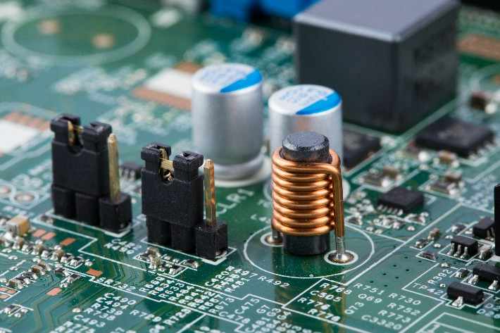
Test materials and equipment
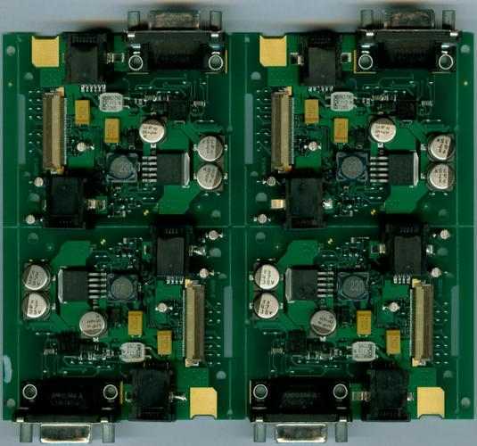
LTCC circuit Board: The multi-layer circuit board is sintered by Ferro A6-S raw ceramics, the size is 80mm x 30mm x 1.2mm, the component shell material is Kovar alloy, the box wall thickness is 1.0mm, the bottom size is 80mm x 30mm, and the bottom thickness is 2.0mm. Solder is Sn63Pb37 sheet 0.1mm thick.
Test equipment: Self-made nitrogen-filled glove box with heating table, rated working temperature of 450℃.
X-ray testing equipment: MACROSCIENCE MXR-160.
Digital camera equipment: OLYMPUS MODEL NO. C5060.
LTCC circuit board surface metallization method:
At present, there are two kinds of metallization methods for LTCC subgrade plate: thick film sintering method and sputtering film plating thickening method. Although the sputtering film replating thickening method has been widely used in the thin film circuit processing of single layer ceramic substrate. But the LTCC circuit board is still in the exploratory phase. At present, the general method to improve the welding resistance of LTCC circuit boards is to sintering a layer of palladium silver.
Welding resistance test method:
Three kinds of samples were selected to compare the welding resistance: (1) thick film palladium silver layer (about 12μm) sample; (2) thick film gold layer (about 37μm) sample; (3) A composite metal film (about 10μm) containing Ni Barrier layer 3(Nj+ m) was set up. M was the metal code.
Refer to GJB548A-96 (Test Methods and Procedures for Microelectronic Devices) : The substrate was vertically immersed in the tin tank of molten solder at (215±5) ℃, 58 times each time, 10 times in total (the solder composition is 63Sn37Pb eutectic solder, the flux is 25% rosin alcohol solution) to clean and apply flux. The inspected graph should have no warping, falling off, breaking, melting erosion area of less than 20%. All of the above three samples can pass the test and test standards of welding resistance, and no places are observed to be corroded. Then, solder pads coated with flux are placed on the surface of the metallized layer of the above three samples (new samples). Under nitrogen protection, they are heated and maintained on the hot table at 240℃ (set value) to observe the corrosion on the surface of the metallized layer of the corresponding samples of solder.
LTCC circuit board and box body gas welding method:
The methods that can realize the large-area brazing between the LTCC subgrade plate and the bottom of the box include gas shielded brazing, vacuum brazing and hot plate brazing in air. The corresponding soft brazing material in the air is more likely to react with oxygen in the air when it is in liquid state, so the gas shielded brazing has obvious advantages over the hot plate brazing in the air. However, gas brazing and vacuum brazing have their own advantages and disadvantages. The heat conduction in vacuum mainly depends on radiation and the shielding effect is obvious. Due to the small size of the microwave element, the temperature on each workpiece is not uniform, resulting in high temperature of some workpiece, excessive solder flow, and insufficient temperature of some workpiece. Incomplete melting and spreading, poor consistency of brazing quality, long heating cycle, low efficiency.
Three kinds of heat conduction coexist in gas shielded brazing, which is convenient to operate and high efficiency, but the brazing rate is limited due to the existence of gas. Under normal conditions, it can reach more than 75%, showing random distribution. For microwave circuits, it brings great uncertainty. In order to improve the brazing rate, the method of pre-setting "convex spot" is used. The salient is made of the same material as the weld material for large area brazing. Convex points are made by placing an appropriate amount of solder paste in the corresponding position and forming convex points through hot air reflux. The size of the bumps varies with the length of the substrate. After the convex spot is made, a weld with the same composition as the oxide skin and the convex spot is pre-arranged at the bottom of the box body. Large area ground welding between LTCC and bottom of box is achieved by heating on hot plate protected by gas.
Brazing rate test:
After brazing a large area, the solder should theoretically fill as much space as possible between the LTCC and the bottom of the box using the principle of capillarity. But because of the protective atmosphere, the molten solder randomly forms multiple rings, trapping the gas inside. If there is a cavity inside the brazing interface or the solder alloy is loosened during solidification, the X-ray is easy to pass through, resulting in white or off-white bright spots in the imaging image. The X-ray scan of the "convex spot" welding process is not set, the arrow indicates the obvious welding defect, the brazing rate is about 75%, the X-ray scan of the "convex spot" welding process is set. Arrows indicate minor welding defects, brazing rates above 98%. Due to the presence of "bumps", the temperature difference between the two ends of the LTCC substrate was artificially caused during heating. The slow collapse of the "bumps" facilitates the removal of inclusion gases between the solder at the bottom of the box and the LTCC substrate. X-ray images show that the brazing rate can be improved by designing "bumps" on the welding surface of the matrix under gas protection.
LTCC circuit board large area ground brazing Conclusion:
(1) By setting (Ni+M) composite metal film layer, the welding resistance of large area metallized layer of LTCC substrate to Sn63Pb37 solder is greatly improved, ensuring the reliable brazing of LTCC substrate and box body;
(2) Using gas protection, the design of "bumps" on the welded surface of the LTCC substrate is very effective in improving the brazing rate between the LTCC subgrade board and the box body.


Just upload Gerber files, BOM files and design files, and the KINGFORD team will provide a complete quotation within 24h.