
Professional PCB manufacturing and assembly
Building 6, Zone 3, Yuekang Road,Bao'an District, Shenzhen, China
+86-13410863085Mon.-Sat.08:00-20:00


Miniaturization has made it more difficult to align multiple connectors, and pursuing optimal design practices and talking to connector providers early can help ensure design success
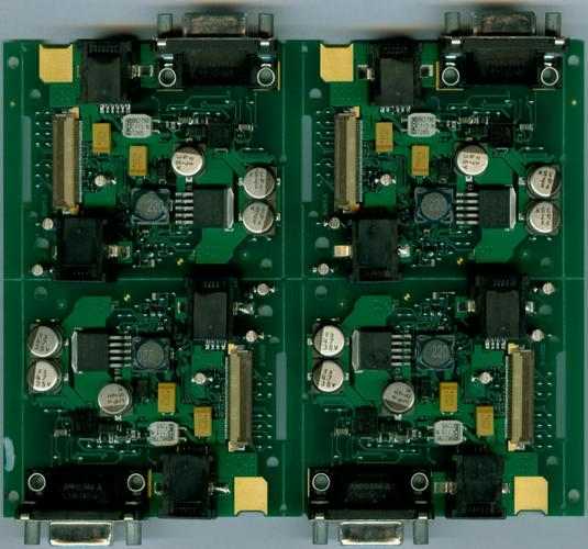
Manufacturers of printed circuit boards (PCB boards) are under significant pressure to increase density, reduce space occupancy, reduce side dimensions, manage heat flow and improve data rates while improving reliability and reducing costs. As they continue to successfully reduce these pressures, an interesting challenge arises for designers to align multiple paired connector groups between two PCB boards.
What is needed are clear guidelines to understand how to meet these alignment challenges without sacrificing system performance, density, and reliability, while meeting increasingly stringent budget and time-to-market requirements.
This article discusses the challenges of alignment in more detail before describing the conflicting requirements that may be encountered between advanced PCBS and more reliable high-density connectors so that these requirements can be met efficiently using design best practices.
Miniaturization makes connector alignment difficult
There are many directions in which PCB boards can be improved, including density, higher data rates, thermal management, and reliability. Along with these improvements, however, is the pressure that the trend toward miniaturization puts on designers in terms of connector selection and implementation, especially pairing multiple connectors to PCB boards.

In the case of connectors, over the past 25 years, miniaturization has led to a drop in spacing from 0.100 inches (2.54 mm) to 0.016 inches (0.40 mm) -- that's a sixfold reduction, requiring tighter tolerances. However, tighter tolerances are not the problem per se, but rather the variability around the nominal tolerances: if multiple connectors change to any of the nominal limits, some problems are more likely to occur.
Applications using a single paired connector group do not present problems: Because there is no tolerance accumulation, the sandwich card is assumed to float freely, and the connector's global and local alignment capabilities will ensure perfect alignment.
Applications that use a single paired connector (top) have no stacking tolerances, and the connector's global and local alignment capabilities will ensure perfect alignment. Multiple connectors introduce errors, and these tolerances can add up and cause alignment errors.
However, adding more paired groups of connectors to the same female sandwich card in any direction and at any distance introduces some cumulative tolerances (Figure 2, bottom). These tolerances are particularly important for PCB workshops, electronic manufacturing services, and the properties of the materials used in PCB boards.
To illustrate this, consider using a multi-sandwich connector system. This assembly consists of six or more components: motherboard (A), sandwich card (B), female connector # 1 (C), paired with male connector # 1 (D), and female connector #2 (E), paired with male connector #2 (F).
An unlimited number of connectors can be successfully deployed between two PCBS provided that sandwich connectors and sufficiently rigid PCB boards can be manufactured, machined, and assembled in precisely nominal conditions; In fact, tolerance and variability of material properties are limiting or decisive factors. In the case shown in Figure 2, the designer needs to consider and account for the tolerances of all components, including (A) and (B) two often overlooked but related tolerances for PCB boards.
How do I solve the PCB board-to-connector alignment problem
The procurement of certain PCB boards is controlled only by the specifications embedded in the Gerber packet. PCB boards can be built from these packets, regardless of mechanical tolerances.
: Some PCB board procurement items are controlled only by the specifications embedded in the Gerber package, so that the PCB board can be built according to these packages without regard to mechanical tolerances. For multi-connector applications, this packet needs to be used with a separate mechanical drawing.
For multi-connector applications, this packet must be accompanied by a separate mechanical drawing indicating the original drawing, drilling, and wiring tolerances.
At this point, the designer needs to do two things to help ensure a successful outcome. The first step is to find out what support PCB board vendors and connector vendors can provide to ensure alignment. The second is to ensure that system-level tolerances have been studied to determine connector alignment deviations resulting from their design.
With A multi-connector sandwich card system consisting of A to F components, the connector supplier can only control the connector tolerances. A good supplier will meet or exceed published performance specifications, make PCB board tolerances and machining recommendations, and even provide referrals for recommended PCB suppliers and equipment as required.
The system or product designer should refer to the connector placeholder dimensions and product specifications. The alignment deviation specifications contained in these documents should be compared with the results of system-level tolerance studies to help ensure that multiple connectors between the same board are used successfully.
As long as the initial and final angles and linear alignment deviations are not exceeded, the connector system should function properly. These alignment deviation values are calculated by taking into account factors such as insulator interference, beam deflection, and contact friction. Exceeding the alignment deviation may result in circuit and/or insulator disconnection or damage.
While all the necessary information about design, component tolerances, equipment, and manufacturing capabilities is usually readily available to the designer, it is important to be able to contact the connector manufacturer to provide more specific guidance and verification of alignment deviation tolerance accumulation.


Just upload Gerber files, BOM files and design files, and the KINGFORD team will provide a complete quotation within 24h.