
Professional PCB manufacturing and assembly
Building 6, Zone 3, Yuekang Road,Bao'an District, Shenzhen, China
+86-13410863085Mon.-Sat.08:00-20:00

In recent years, the market demand for high-rise board in application communication, base station, aviation, military and other fields is still strong, and with the rapid development of China's telecom equipment market, the prospect of the high-rise board market is promising.
At present, the domestic PCB manufacturers that can mass produce high - level circuit boards mainly come from foreign enterprises or a few domestic enterprises. The production of high-level circuit board not only needs higher technology and equipment investment, but also needs more experience accumulation of technical personnel and production personnel. At the same time, the import of high-level board customer certification procedures are strict and cumbersome, so the high-level circuit board entering the enterprise threshold is higher, and the realization of industrial production cycle is longer.
The average number of PCB layers has become an important technical index to measure the technical level and product structure of PCB enterprises. This paper briefly describes the main processing difficulties encountered in the production of high-rise circuit boards, introduces the control points of the key production processes of high-rise circuit boards, for your reference.
First, the main production difficulties
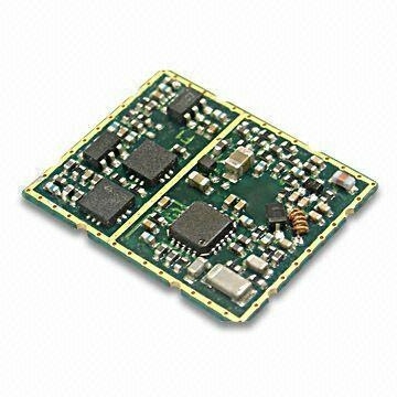
Compared with the characteristics of conventional circuit boards, high-rise circuit boards have thicker, more layers, denser lines and holes, larger unit size, thinner dielectric layer, and more stringent requirements for inner space, interlayer alignment, impedance control and reliability.
1. Difficulty in interlayer alignment
Due to the number of high-rise board layers, the customer design end of PCB layer alignment requirements are more and more strict, usually the inter-layer alignment tolerance control ±75μm, considering the large size design of high-rise board units, graphic transfer workshop ambient temperature and humidity, as well as different core board layer growth and shrinkage inconsistency caused by dislocation superposition, inter-layer positioning mode and other factors. It makes it more difficult to control the alignment degree between the layers of the high floor.
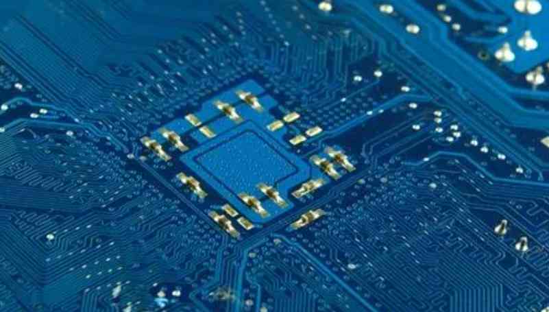
2. Difficulties in making inner circuits
High TG, high speed, high frequency, thick copper, thin dielectric layer and other special materials are used in high-rise board, which puts forward high requirements for inner line fabrication and graphic size control. For example, the integrity of impedance signal transmission increases the difficulty of inner line fabrication. Line width line distance is small, open short circuit increase, micro short increase, low qualified rate; There are more signal layers in the fine line, and the probability of missing AOI in the inner layer increases. Inner core plate thickness is thin, easy to fold resulting in poor exposure, etching machine is easy to roll plate; Most of the high-rise boards are system boards, the unit size is large, and the cost of scrap in finished products is relatively high.
3. Difficulties in pressing and making
The superposition of multiple inner core plates and semi-cured sheets is easy to produce defects such as slide plate, delamination, resin cavity and bubble residue during pressing production. In the design of laminated structure, it is necessary to fully consider the heat resistance, voltage resistance, filling amount and medium thickness of the material, and set a reasonable high layer plate pressing program. Because of the large number of layers, the volume control and size coefficient compensation cannot be consistent. The thin insulation layer between layers is easy to cause the failure of inter-layer reliability test.
4. Difficulties in drilling
Special plates of high TG, high speed, high frequency and thick copper are used to increase the roughness of drilling, burr of drilling and the difficulty of removing drilling dirt. The number of layers, the cumulative total copper thickness and plate thickness, drilling easy to break the knife; CAF failure caused by dense BGA and narrow pore wall spacing; The thickness of the plate is easy to lead to the problem of oblique drilling.
Two, Control of key production processes
1. Material selection
With the development of electronic components in the direction of high performance and multi-function, it also brings high frequency and high speed signal transmission. Therefore, low dielectric constant and dielectric loss of electronic circuit materials are required, as well as low CTE, low water absorption and better high-performance copper clad plate materials, in order to meet the processing and reliability requirements of high-rise board. For the high thickness copper circuit board, the semi-cured sheet with high resin content is selected. The flow glue amount of the semi-cured sheet between layers is enough to fill the inner layer pattern. If the insulating medium layer is too thick, the finished board is easy to be super thick.
2. Compacted laminated structure design
The main factors considered in the design of laminated structure are the heat resistance, voltage resistance, filling amount and dielectric layer thickness of the material, which should follow the following main principles.
(1) The manufacturer of semi-cured sheet and core plate must be consistent. In order to ensure PCB reliability, 1080 or 106 semi-cured sheets shall be avoided for all layers (except for special requirements of the customer). If the customer has no requirement of medium thickness, the thickness of medium between each layer shall be guaranteed to be ≥0.09mm according to IPC-A-600G.
(2) When the customer requires high TG plate, the core plate and semi-cured plate shall use the corresponding high TG material.
(3) Inner substrate 3OZ or above, select high resin content of semi-cured tablets, such as 1080R/C65%, 1080HR/C 68%, 106R/C 73%, 106HR/C76%; However, the structural design of 106 high-adhesive semi-cured sheets should be avoided as far as possible, so as to prevent multiple pieces of 106 semi-cured sheets from overlapping. Because the glass fiber yarn is too thin, the glass fiber yarn will collapse in the large substrate area, which will affect the dimensional stability and burst plate stratification.
(4) If the customer does not have special requirements, the thickness tolerance of the dielectric layer between layers is generally controlled by +/-10%. For impedance plates, the thickness tolerance of the dielectric layer is controlled by IPC-4101 C/M class tolerance. If the influence factor of impedance is related to the thickness of the substrate, the plate tolerance must also be controlled by IPC-4101 C/M class tolerance.
3. Interlayer alignment control
The precision of inner core board size compensation and the control of production size requires accurate compensation of each layer graphic size of high-rise board through the data and historical data experience collected during production for a certain period of time, so as to ensure the consistency of each layer core board growth and shrinkage. Select high precision, high reliability before pressing interlayer positioning methods, such as four slot positioning (Pin LAM), hot melt and rivet bonding. The key to ensure the pressing quality is to set up the appropriate pressing process and daily maintenance of the press, control the merging glue and cooling effect, and reduce the dislocation between layers. The control of interlayer alignment degree should be considered from the compensation value of inner layer, the pressing positioning mode, the pressing process parameters, the material characteristics and other factors.
4. Inner line process
Since the resolution capacity of the traditional exposure machine is about 50μm, the laser direct imaging machine (LDI) can be introduced for the production of high-rise plate to improve the graphic resolution capacity to about 20μm. The alignment accuracy of conventional exposure machine is ±25μm, and the alignment accuracy between layers is greater than 50μm. Using high precision alignment exposure machine, graphic alignment accuracy can be improved to about 15μm, interlayer alignment accuracy control within 30μm, reduce the alignment deviation of traditional equipment, improve the interlayer alignment accuracy of high layer board.
In order to improve the etching ability of the line, the need in the engineering design of the width of the line and the welding plate (or ring) to give appropriate compensation, but also need to special graphics, such as back circuit, independent line compensation amount to do more detailed design considerations. Confirm whether the design compensation for inner line width, line distance, isolation ring size, independent line, hole to line distance is reasonable, otherwise modify the engineering design. Impedance, inductive design requirements pay attention to independent line, impedance line design compensation is enough, etch control parameters, the first confirmed qualified before mass production. In order to reduce etching side erosion, it is necessary to control the composition of each group of etching solution within the best range. The traditional etching line equipment has insufficient etching ability, so it can be reformed or imported with high precision etching line equipment to improve the etching uniformity and reduce the problems of etching rough edge and unclean etching.
5. Pressing process
At present, interlayer positioning methods before pressing mainly include: four-slot positioning (Pin LAM), hot melt, rivet, hot melt and rivet combination. Different product structures adopt different positioning methods. For the high level plate using four slot positioning mode (Pin LAM), or using fusion + riveting production, OPE punching machine out of the positioning hole, punching accuracy control in ±25μm. In the fusion adjustment mechanism, X-RAY should be used to check layer skewness for the first plate, and the layer skewness can be qualified before batch production. During batch production, it is necessary to check whether each plate is fused into the unit to prevent subsequent stratification. The pressing equipment uses a high-performance supporting press to meet the inter-layer alignment accuracy and reliability of high-rise plates.
According to the laminated structure of the high-rise board and the materials used, the appropriate pressing procedure is studied, and the optimal heating rate and curve are set. On the conventional pressing procedure of the multilayer circuit board, the heating rate of the pressing board is appropriately reduced, and the high temperature curing time is extended, so that the resin can fully flow and cure, and at the same time, the problems of sliding plate and interlayer dislocation in the pressing process are avoided. Material TG value is not the same as the plate, can not be with the grate plate; The plate with ordinary parameters can not be mixed with the plate with special parameters; The performance of different sheets and semi-cured sheets is different. The corresponding sheet semi-cured sheet parameters should be used for pressing. The special materials that have never been used need to verify the process parameters.
6. Drilling process
Due to the superposition of each layer, the plate and copper layer are too thick, which causes serious wear to the drill bit and is easy to break the drill tool. The number of holes, falling speed and rotating speed should be adjusted appropriately. Accurately measure the expansion and contraction of the plate to provide accurate coefficient; The number of layers is more than 14 layers, the aperture is less than 0.2mm or the distance from the hole to the line is less than 0.175mm, and the drilling machine with the accuracy of the hole position is less than 0.025mm is used for production. The diameter above φ4.0mm is drilled by steps, the thickness to diameter ratio is 12:1 is drilled by steps, positive and negative drilling method; Control the drilling edge and hole thickness. Adopt new drilling tool or grind 1 drilling tool to drill the upper board as far as possible, and control the hole diameter within 25um. In order to improve the drilling burr problem of high-rise thick copper plate, the batch verification, the use of high-density plate, the number of laminated plates is one piece, the drill grinding time is controlled within 3 times, can effectively improve the drilling burr.
Backdrilling technology is an effective way to improve signal integrity for high frequency, high speed and mass data transmission. The back drilling controls the length of the residual stub, the consistency of the two holes, and the copper wire in the holes. Not all drilling equipment has backdrilling function. You must upgrade the technology of drilling equipment (with backdrilling function) or purchase a drilling machine with backdrilling function. Back drilling techniques applied from industry literature and mature mass production mainly include: traditional deep-controlled back drilling method, back drilling with signal feedback layer in the inner layer, and calculating depth back drilling in proportion to plate thickness.
Three. Reliability test
The high-rise board is generally the system board, thicker than the conventional multilayer board, heavier, larger unit size, the corresponding heat capacity is also larger, in the welding, the need for more heat, the welding experience of high temperature for a long time. At 217℃(melting point of solder), it takes 50 to 90 seconds, and the cooling rate of the high-rise plate is relatively slow, so the over-reflow test time is extended, and combined with IPC-6012C, IPC-TM-650 standards and industry requirements, the main reliability test of the high-rise plate.


Just upload Gerber files, BOM files and design files, and the KINGFORD team will provide a complete quotation within 24h.