
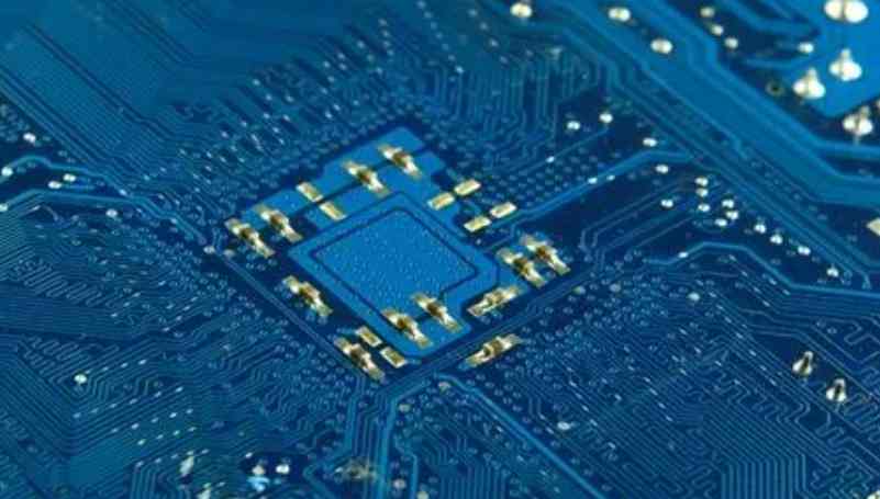
Professional PCB manufacturing and assembly
Building 6, Zone 3, Yuekang Road,Bao'an District, Shenzhen, China
+86-13410863085Mon.-Sat.08:00-20:00

Designers may design odd-layer printed circuit boards (PCBS). If wiring doesn't require an extra layer, why use it? Wouldn't reducing layers make the board thinner? Wouldn't it cost less if the board had one less layer? However, in some cases, adding a layer can actually lower the cost.
The circuit board has two different structures: core structure and foil structure.
In the core structure, all the conductive layers in the circuit board are coated on the core material; In the foil-coated structure, only the internal conductive layer of the circuit board is applied to the core material, and the external conductive layer is applied to the foil dielectric plate. All conductive layers are bonded together by a medium using a multilamination process.
Nuclear material is double-sided foil in a factory. Because each core has two sides, the PCB has an even number of conductive layers when fully utilized. Why not use foil on one side and nuclear structure on the rest? The main reasons are: the cost of PCB and PCB bending degree.
Cost advantage of even layer circuit boards
Because there is one less layer of medium and coating foil, the cost of odd-numbered PCB board raw materials is slightly lower than that of even-numbered PCB board. But the processing cost of odd layer PCB is obviously higher than that of even layer PCB. The inner layer has the same processing cost; However, the foil/core structure significantly increases the processing cost of the outer layer.
Odd layer PCB needs to add non - standard laminated core layer bonding technology on the basis of nuclear structure technology. Compared with the nuclear structure, the production efficiency of the plant adding foil outside the nuclear structure will decrease. Prior to laminating, the outer core requires additional processing, which increases the risk of scratches and etching errors on the outer layer.
The best reason not to design PCBS with odd layers is that they bend easily. When the PCB is cooled after the multilayer circuit bonding process, the different lamination tension between the core structure and the foil-coated structure can cause the PCB to bend. As the board thickness increases, the risk of bending becomes greater for composite PCBS with two different structures. The key to eliminate circuit board bending is to use balanced layering. Although the PCB with a certain degree of bending meets the requirements of the specification, the subsequent processing efficiency will be reduced, resulting in an increase in cost. Because assembly requires special equipment and technology, the accuracy of component placement is reduced, so the quality will be damaged.
Use an even number of PCB layers
When an odd number of PCB layers appear in the design, the following methods can be used to balance the layering, reduce the cost of PCB production, and avoid PCB bending. The following methods are listed in order of preference.
1. A signal layer and use. This method can be used if the PCB is designed with even power layers and odd signal layers. The additional layer does not increase the cost, but can shorten the lead time and improve PCB quality.
2. Add an additional power layer. This method can be used if the PCB is designed with odd power layers and even signal layers. An easy way to do this is to add a layer in the middle of the stack without changing the other Settings. Route an odd number of PCB layers first, then duplicate layers in the middle and label the remaining layers. This is the same electrical property as the coating of thickened layers.
3. Add a blank signal layer near the center of the PCB stack. This method minimizes cascade unbalance and improves PCB quality. The odd-numbered layers are routed, and a blank signal layer is added to mark the remaining layers. In microwave circuits and mixed media (media with different permittivity) circuit types are used.
Balanced laminated PCB advantages: low cost, not easy to bend, shorten delivery time, ensure quality.
PCB circuit boards and electromagnetic compatibility of the design steps
The rapid development of mobile phone, electronics, communication industry, but also promote the PCB circuit board industry is growing and growing rapidly, people for the components of the layer, weight, precision, materials, color, reliability and other requirements more and more high.
However, due to the fierce price competition in the market, the cost of PCB board materials is also on the rise. In order to improve the core competitiveness, more and more manufacturers monopolize the market with low prices. However, behind these ultra-low prices, is to reduce the cost of materials and production costs to obtain, but the device is usually prone to cracks (cracks), easy scratches, (or bruises), its precision, performance and other comprehensive factors are not up to standard, seriously affecting the use of products on the weldability and reliability and so on.
In the face of various PCB circuit boards on the market, distinguish PCB circuit boards good or bad can start from two aspects; The first method is to judge from the appearance, on the other hand is to judge from the quality specification of PCB board itself.
First: Distinguish from the appearance of the circuit board is good or bad (in general, the appearance of the PCB circuit board can be analyzed through three aspects;
1. Standard rules for size and thickness. The thickness of the circuit board to the standard circuit board is different sizes, customers can measure and check according to their own product thickness and specifications.
2. Light and color. External circuit boards are covered with ink, circuit boards can play the role of insulation, if the color of the board is not bright, less ink, insulation board itself is not good.
3. Appearance of weld. Due to more parts of the circuit board, if the welding is not good, parts easy to fall off the circuit board, seriously affect the welding quality of the circuit board, good appearance, careful identification, the interface is very important.

Second: high-quality PCB circuit boards need to meet the following requirements
1. The telephone should be easy to use after the components are installed, that is, the electrical connection should meet the requirements;
2, line width, line thickness, line distance meet the requirements, so as to avoid line heating, open circuit, and short circuit;
3, by high temperature copper is not easy to fall off;
4, the surface of copper is not easy to oxidize, affect the installation speed, oxidation after use soon after bad;
5. No additional electromagnetic radiation;
6. The shape is not deformed, so as to avoid the deformation of the shell and dislocation of the screw hole after installation. Now are mechanized installation, circuit board hole location and line and design deformation error should be within the allowable range;
7, and high temperature, high humidity and special environment should also be considered in the range;
8. The mechanical properties of the surface should meet the installation requirements.


Just upload Gerber files, BOM files and design files, and the KINGFORD team will provide a complete quotation within 24h.