
Professional PCB manufacturing and assembly
Building 6, Zone 3, Yuekang Road,Bao'an District, Shenzhen, China
+86-13410863085Mon.-Sat.08:00-20:00

There are many exquisite PCB presets, whether it is the principle of presets or components mix and match, are strict requirements. So what is not easy to solve about the factory process of multilayer circuit board?
PCB multilayer circuit boards are generally defined as 10-20 or more advanced multilayer circuit boards. They are more difficult to process than traditional multilayer circuit boards, and they require high quality and reliability. Mainly used in communication facilities, high-end servers, medical electronics, aviation, industrial control, military and other fields. In recent years, the market demand of high-rise board in communication, base station, aviation, military and other fields is still strong.
PCB uniform level has become a balance PCB company technical level static product structure of the close technical index. In this paper, the main processing problems encountered in the production of high rise circuit board are described briefly, and the key points of controlling the key production technology of multi-layer circuit board are introduced for reference.
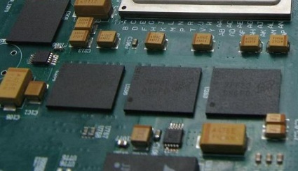
In contrast to traditional PCB products, high-rise PCB circuit boards have many unique features such as thick board, multiple layers, dense lines, multiple holes, large unit size, thin media layer, etc., and high requirements for inner and inner space, inter-layer aiming, impedance control and reliability.
1. It is not easy to solve the problem between layers
Because of the large number of high - level panels, users have higher and higher requirements for PCB layer calibration. Generally, the sighting tolerance between layers is choke to 75 microns. Considering the problem to the high level circuit board unit size, graphic change workshop background temperature and humidity degree is large, different core board is not exactly the same cause of dislocation layering, interlayer positioning form, to get the high level board more difficult to control.
2, the inner circuit manufacturing is not easy to solve
The high level circuit board is considered appropriate and uses high TG circuit board, high speed circuit board, high frequency circuit board, thick copper circuit board, thin media layer and other special materials, the inner circuit manufacturing and graphic size control makes the request tall. For example, the integrity of the transmission of impedance signals increases the difficulty of making inner circuits.
Width and line spacing is small, open circuit and short circuit increase, short circuit increase, low standard rate; With many thin line signal layers, the probability of AOI leakage detection in the inner layer increases. The inner core plate is thin, easy to wrinkle, exposure is not good, easy to curl when etching machine; The high level plate is mostly system plate, the unit size is large, and the product waste cost is high.
3, compression production is not easy to solve
Many inner core plates and semi-cured plates are superimposed, which are easy to reveal in the stamping production of skateboards, stratification, natural resin holes and bubbles. In the presetting of lamination structure, it is necessary to fully consider the heat resistance, pressure resistance, adhesive content and dielectric thickness of the problem material, and formulate a reasonable suppression scheme of high rise sheet metal.
Because of the number of layers, expansion and shrinkage choke and size coefficient repayment can not maintain exactly the same, thin layer insulation is easy to cause the failure of inter-layer reliability attempt.
4, drilling manufacturing is not easy to solve the place
The use of high TG circuit boards, high speed circuit boards, high frequency circuit boards and thick copper circuit boards as appropriate increases the difficulty of drilling smoothness, drilling burr and drilling dirt removal. Many layers, total copper thickness and plate thickness, drilling easy to break the knife; The loss of effectiveness of CAF caused by dense BGA and narrow pore wall spacing; The thickness of the plate is easy to cause the problem of oblique drilling.


Just upload Gerber files, BOM files and design files, and the KINGFORD team will provide a complete quotation within 24h.