
Professional PCB manufacturing and assembly
Building 6, Zone 3, Yuekang Road,Bao'an District, Shenzhen, China
+86-13410863085Mon.-Sat.08:00-20:00

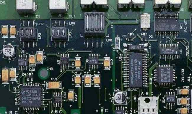
The PCB boarditself is made of insulating, heat-resistant, and non-bendable material. The small wire material that can be seen on the surface is copper foil. Originally, copper foil is covered on the whole board, but in the manufacturing process, the middle part is etched away, and the remaining part becomes a network of small lines. These lines are called wires or wiring, and are used to provide circuit connections for the components on the PCB board. Usually the color of PCB board is green or brown, which is the color of solder resistance. It is an insulating protective layer, which can protect copper wire, prevent short circuit caused by wave welding, and save the amount of solder. A screen printing surface is also printed on top of the solder resistance layer. It is usually printed with words and symbols (mostly white) to indicate the position of the parts on the board. Screen printing surface is also known as icon surface. In the final product, integrated circuits, transistors, diodes, passive components (resistors, capacitors, connectors, etc.) and a variety of other electronic components are installed. Through wire connection, can form electronic signal connection and function.
So PCB processing needs to consider PCB size, PCB shape, clamping edge, MARK point and other aspects. Because high quality circuit boards are produced by using qualified raw materials through strict and reasonable process, inspection is only through inspection, select qualified products, pick out defective products and waste products, quality management in the process of PCB processing is the core part to ensure quality.
1. Bad size
There are many possible reasons for the poor size of the circuit board. The PCB processing process is prone to shrinkage and expansion. The PCB manufacturer has adjusted the drilling procedure, graphic proportion and molding CNC procedure, which may lead to the easy deviation of the mounting and poor coordination of the structural parts. Because such problems are difficult to check out, it can only rely on the PCB manufacturer's good processing process control, so special attention should be paid to the selection of PCB manufacturers.
2. The board is bent and warped
The reasons that may lead to the bending and warping of the circuit board include material problems, abnormal processing process, poor processing control, improper transportation or storage, inadequate fracture hole design, and large differences in the copper area of each layer. Design problems need to be avoided in the early stage of design review, and PCB manufacturers are required to simulate the IR conditions for the test, so as to avoid the bad bending of the plate after passing the furnace. For some sheets, the wood pulp board can be pressed up and down during packaging before packaging to avoid subsequent deformation. At the same time, fixture can be added during SMT to prevent the device from bending the board under excessive pressure.
3. Bad plug hole
The poor plug hole of circuit board is mainly caused by the insufficient process capacity of PCB manufacturers or the simplified process, which is manifested as the plug hole is not full, the hole ring has exposed copper or false exposed copper. May cause insufficient solder, short circuit with SMT patch or assembly device, residual impurities in the hole and other problems. This problem can be found in appearance inspection, so it can be controlled in incoming inspection, and PCB processing manufacturers are required to improve it.
4. Bad impedance
The impedance of circuit board is an important index related to the radio frequency performance of circuit board. The common problem is that the impedance difference between circuit board batches is relatively large. As the impedance test strips are usually made on the edge of PCB circuit board, and will not be shipped with the circuit board, PCB manufacturers can be asked to attach the impedance strips and test report of this batch for reference each time they ship, and also ask to provide the comparison data of the edge diameter of the board and the inner diameter of the board.
5, poor hole breakage
It comes from the poor treatment of the slag removal process. In the processing of PCB circuit board, the slag removal process will first be treated with leaven agent, and then the erosion operation of strong oxidant "permanganate", this process will remove the slag and produce microporous structure. After the removal process of residual oxidizer, rely on reducing agents to remove, typically using acidic liquid treatment. Because there will be no residual slag problem after slag treatment, we often ignore the monitoring of reducing acid, which may allow the oxidizer to remain on the pore wall. After the circuit board into the chemical copper process, after the whole hole agent treatment of the circuit board will be micro corrosion treatment, then the residual oxidizer is again acid soaked and let the residual oxidizer resin peel off, but also equal to the destruction of the whole hole agent. The damaged pore wall will not react in the subsequent palladium colloid and chemical copper treatment, and these areas show no copper precipitation phenomenon. The foundation is not established, of course, electroplated copper can not be covered completely and produce punctured holes. This kind of problem has occurred in many circuit board factories in circuit board processing, pay more attention to the removal of glue slag process reduction steps potion monitoring should be able to improve. Every link of PCB circuit board processing needs our strict control, because chemical reactions sometimes occur slowly in the corners we do not pay attention to, thus destroying the entire circuit.


Just upload Gerber files, BOM files and design files, and the KINGFORD team will provide a complete quotation within 24h.