1. The installation of decoupling capacitor and PCB design
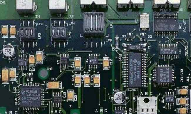
When installing decoupling capacitors, it is generally understood to make the capacitor's leads as short as possible. However, in practice, it is often limited by installation conditions, and the lead of the capacitor cannot be obtained very short. Moreover, the parasitic inductance of the capacitor itself is only one of the factors affecting the self-resonant frequency, which is also related to the parasitic inductance of the through hole pad, the parasitic inductance of the related printed conductor and other factors. In practical application, it is not only difficult to pursue the short lead, but also may not achieve the purpose. When the location of the decoupling capacitor on the PCB is not possible to use a very short printed lead, the printed line must be bolded.
Practice has proved that a printed wire with aspect ratio less than 3 has very low impedance and can meet the requirements of decoupling capacitor lead. Of course, the number of holes should be reduced as far as possible, and the parasitic inductance of holes should be reduced as far as possible when designing holes.
2. Design method of capacitor bypass
Bypass in EMC can be understood as the drainage of unnecessary common-mode RF energy from a component, circuit, or cable. It essentially generates an AC branch to deflect unwanted energy away from susceptible areas, and it also provides a filter function that is usually limited by the bandwidth of the device. Therefore, it can also be called filtering in a sense.
Bypasses usually occur between power sources and ground, signals and ground, or between different ground. It is different from the essence of decoupling, and the use of capacitors is the same. In EMC, bypass is also colloquially known for its role in changing the path of a common-mode current or providing an additional current path to a common-mode voltage.
The indirect bypass capacitance between the ground of the analog circuit and the ground of the product is 10nF, usually during EMC testing and rectification. If the EFT/B test of the product cable is carried out, it will change the main path of the injected interference current flowing inside the product, so that most of the interference current flows from the bypass capacitor to the earth, so that the common mode current flowing through the sensitive circuit is greatly reduced, so as to protect the sensitive circuit, the EFT/B interference degree level can be greatly improved.
Note: The ground impedance of the bypass capacitor is very important and must be very small. If PCB wiring is used, PCB copper wiring with aspect ratio less than 3 has a very small impedance, less than 4 Ω at 100MHz frequency.
In the typical radiation case of EMC testing and rectification, common-mode voltage parasitic between analog circuit and digital circuit is the main reason for the formation of common-mode radiation. Bridging a bypass capacitor that is much larger than the parasitic capacitor between the ground of the analog circuit and the ground of the digital circuit, or between the primary stage of the isolating transformer in a switching power supply circuit, acts as an additional current shunt path to the common-mode voltage source of common-mode radiation, reducing the common-mode current flowing into the connecting line cable (which is typically a transmitting antenna). In EMC design, it can be concluded that the bypass capacitor has two main functions:
1) Guide the common mode current to the safe area. Including guiding the common-mode interference current in the injection cable to flow to the reference ground floor or ground, metal shell in the product, metal plate, etc., can make the common-mode interference current flow to the safe area. The internal sensitive devices and circuits in the product are protected, and the common mode current generated by the noise circuit inside the product is limited to a safer area, so that the EMI common mode current does not flow to the cable and interface. This security zone is defined as an area where EMC problems do not occur.
2) Provide a high-frequency channel, which can realize circuit isolation at both ends of the bypass capacitor at DC or low frequency, and realize interconnection at high frequency, that is, provide a high-frequency channel.

3. X capacitance and Y capacitance
According to the standard IEC 60384-14 for safety capacitor series used in electronic equipment, capacitors are divided into X capacitors and Y capacitors. In the power supply circuit, AC power input is generally divided into three terminals: live wire (L); Zero line (N); Ground wire (PE). The differential mode capacitance straddled between L and N is the X capacitance; The common-mode capacitor that straddles between L-PE and N-PE at the power supply portion is the Y capacitor. Since the X capacitor has 2 inputs and 2 outputs much like X, it is named the X capacitor. The Y capacitor has an input, an output and a common ground, much like a Y, hence the name Y capacitor.
The X capacitor is mainly used between L and N of the AC power cable. When the X capacitor is used, it is in the open state and does not cause interline short circuit. The X capacitance will be tested for 100 hours at 1.5 times the effective value of the AC voltage, plus at least a 1KV pulse voltage test.
The Y capacitor is mainly used between the L and N of the AC power line and the ground wire, or between the common ground and the shell ground of other circuits. Failure and short circuiting of capacitors straddled to these locations can cause shock hazards especially to the housing connections. The failure mode of the Y capacitor must then be forced to be open circuit. The Y capacitance is tested for 100 hours at 1.7 times the effective value of the AC voltage, plus at least a 2KV pulse high voltage test.
Note: If the connection of Y capacitor is to the earth, it must meet the limit standard of leakage current.
X capacitors are divided into X1, X2 and X3 categories. The main differences are:
1) The high voltage resistance of X1 capacitor is greater than 2.5KV and less than or equal to 4KV.
2) The high voltage resistance of X2 capacitor is less than or equal to 2.5KV.
3) The high voltage resistance of X3 capacitor is less than or equal to 1.2KV.
Y capacitors are further divided into Y1, Y2, Y3 and Y4 categories. The main differences are:
Y1 capacitor can withstand high voltage greater than 8KV.
The Y2 capacitor can withstand high voltage greater than 5KV.
The Y3 capacitor has no special limit to withstand high pressure.
Y4 capacitor can withstand high voltage greater than 2.5KV.


