
Professional PCB manufacturing and assembly
Building 6, Zone 3, Yuekang Road,Bao'an District, Shenzhen, China
+86-13410863085Mon.-Sat.08:00-20:00

As the size of electronic products is getting smaller and smaller, the volume of printed circuit board (PCB) is also shrinking, and the circuit design is becoming more and more intensive. As the power density of components increases, the heat loss of PCB circuit boards is too large, which affects the service life, aging and even failure of components. Embedded copper printed circuit board has the characteristics of high thermal conductivity, high heat dissipation and saving board space, which can effectively solve the heat dissipation problem of high-power electronic components. In this paper, the design of embedded copper PCB and the manufacturing methods of key processes are systematically described from the aspects of embedded copper PCB design, laminated structure, key production technology, product related detection and reliability.
Based on the development of the new generation of information technology, energy-saving and new energy vehicles, electric power equipment and other fields, the solution of the problem of heat dissipation is imminent. At present, there are many ways to solve the problem of PCB board heat dissipation, such as dense heat dissipation hole design, thick copper foil circuit, metal base (core) board structure, embedded copper block design, copper boss design, high thermal conductivity materials. It is one of the effective ways to solve the problem of heat dissipation by directly embedding copper blocks in PCB. However, the existing manufacturing process has some problems, such as insufficient bonding force between copper block and substrate, poor heat resistance, difficult to remove rubber overflow and low qualified rate of products, which limit the application and promotion of embedded copper block PCB technology. Therefore, the existing technology needs to be further studied and improved.
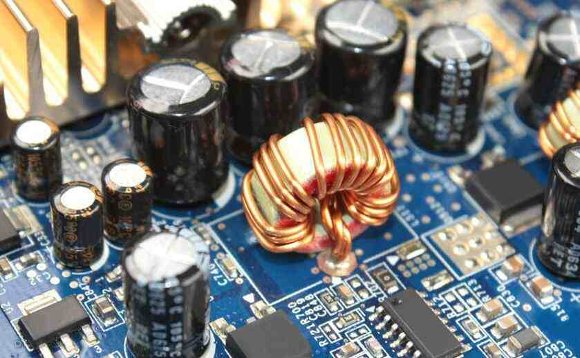
Embedded copper block PCB heat dissipation technology is embedded copper block to FR4 substrate or high frequency mixed pressure substrate, copper thermal conductivity is much greater than the PCB dielectric layer, the power device generated heat can be effectively transmitted through the copper block to PCB and through the radiator. PCB bearing copper block can be designed into multi-layer board, substrate material according to the product structure design needs to choose FR4 (epoxy resin) material or high frequency mixed pressure material. The design of buried copper block is mainly divided into two categories: the first type is semi-buried copper block, named "buried copper block"; The second type is the copper block through type, named "embedded copper block". The thickness of the embedded copper block is less than the total thickness of the plate. One side of the copper block is flush with the bottom layer, and the other side is flush with one side of the inner layer. The thickness of the embedded copper block is close to or equivalent to the total thickness of the plate, and the copper block runs through the top layer. This design has a buried step copper block and a buried straight copper block, and a buried step copper block.Microwave PCB heat dissipation problem has always been one of the more concerned issues in the electronics industry. How to reduce RF (radio frequency) layer thickness, reduce the surface roughness of copper foil at the same time, shorten the heat dissipation path and caloric value, the main way is to improve the thermal conductivity of microwave substrate through technology, intensive heat dissipation hole or local thick copper plating or microwave plate layer thick copper, local embedded heat dissipation copper block. Based on the existing mature microwave plate, the latter two design schemes are usually adopted.
With the continuous improvement of heat dissipation substrate technology and rapid development of the market, heat dissipation substrate in substrate materials and product structure, showing a wave of technical change and innovation. The specific performance is as follows:
(1) Using high thermal conductivity substrate materials, such as aluminum substrate materials, copper substrate materials, metal composite materials, ceramic substrate materials, etc.;
(2) Changes in product structure, such as thick copper foil base plate, metal base (core) plate, embedded copper block plate, ceramic base plate, copper base convex plate, copper conductive column, as well as PCB and heat sink integrated structure of new products.
Laminated structure
Embedded copper PCB board from the laminated structure can be summarized into two categories: the first type is embedded copper block in the FR4 (epoxy resin) material three or more layers of multi-layer structure; The second type is embedded copper block in FR4 core board and high frequency material mixed pressure multilayer board structure.
Manufacturing process of embedded copper block
(1) The size matching of the milling groove between the copper block and the plate (or the mixed pressure area) : the copper block is placed in the milling groove, and the copper block is too loose or too tight, which affects the quality and binding force of the pressing fill.
(2) Flatness control of copper block and plate (or mixed pressure area) : when pressing, flatness of copper block and FR-4 core plate (or mixed pressure area) is difficult to control, it is necessary to ensure that the flatness of copper block and plate is controlled within ± 0.075mm.
(3) The residual glue on the copper block is difficult to remove: when pressing, the residual glue on the copper block is difficult to remove from the overflow resin flow from the gap between the copper block and the plate, which affects the reliability of the product.
(4) Reliability of copper block and plate (or mixed pressure area) : when pressing copper block and FR-4 core plate (or mixed pressure area) there is a certain height difference, easy to lead to the connection of copper block and plate filling insufficient, cavity, crack, stratification and other problems.
Process flow of embedded copper multilayer board
Opening (copper block, FR4 substrate, semi-cured sheet) → inner circuit → inner AOI →OPE punching → inner core plate and semi-cured sheet milling groove → brown → rivet → pressing (placing copper block) → cutting glue (grinding plate) → milling blind groove (controlled depth milling machine) → mechanical drilling (including drilling blind holes) → electroless copper plating → plate electricity → Outer circuit → graphic plating → Outer etching → outer AOI→ welding proof → text → forming → electrical measurement → electroless tin plating → finished product inspection
Process flow of embedded copper block high frequency composite plate
Opening (copper block, FR-4 substrate, high-frequency substrate, semi-cured sheet) → inner circuit (including high-frequency plate) → inner AOI→OPE punching → inner core plate and semi-cured sheet milling groove → brown → rivet → pressing (placing copper block) → cutting rubber (grinding plate) → mechanical drilling (including drilling blind holes) → electroless copper plating → plate electricity → Outer wiring → graphic plating → Outer etching → outer AOI → solder proof → text → molding milling groove → electroless nickel plating/gold → molding → electrical measurement → finished product inspection
The buried copper groove is milled out in the buried copper area of FR4 core plate and semi-cured piece, and then the copper block is browned and pressed together to make the copper block and FR4 core plate together. The processing method of high-frequency material local mixed pressure embedded copper block PCB is to first mill out the buried copper groove and local mixed pressure groove in the mixed pressure area of the inner core board and semi-cured piece buried copper block, then superposition and hot melt, the copper block is embedded in the groove, and then press together, so that the copper block and FR4 substrate and high-frequency substrate are mixed together to achieve the heat dissipation function.
Copper block pressing
Before pressing the copper block, it is necessary to carry out horizontal Browning treatment on the copper block, and use the Browning auxiliary tools (such as mesh dragging plate) to prevent the size of the copper block from being too small, resulting in machine card or falling into the cylinder, to ensure the microerosion effect of the copper block. In order to improve the flatness and reliability of copper block and plate (or mixed pressure area), in addition to considering the matching between copper block thickness and plate thickness, but also choose release film, aluminum sheet, cushion cushion and other appropriate buffer materials, pressing typeset sequence. The lamination structure design is further optimized, the semi-curing sheet with high resin content is selected, and the special pressing program of embedded copper PCB circuit board is set, so that the resin is fully filled and the material is fully cured, to ensure the heat resistance and insulation after pressing.
Copper block forming
There are three main methods for copper block molding: the first is to directly mill out the required size of copper block through a special milling machine, but the need to be equipped with metal substrate milling machine, special milling cutter, high cost; The second is through the secondary processing of the milling machine, with the control of the deep milling function of the milling machine, the use of the double edge milling cutter drill tip shape first rough milling again, and then finish milling again, but need to be equipped with the control of the deep milling function of the milling machine, special milling cutter, the cost is higher; The third is the use of punch cutting, although the production efficiency is high, but the mold production cost is high, the production flexibility is poor, not suitable for sample or small batch production. In order to solve the above problems, the development of graphic etching and milling machine processing technology, the first copper block graphic transfer, and then through the etching machine etching out the shape of copper block, and then the conventional milling cutter, milling machine to the shape of copper block secondary processing, so the production efficiency is higher, the production cost is relatively low.
Inner core plate and semi-cured sheet milling groove
According to the composite structure, the inner groove of the inner core plate and the semi-cured piece is milling. The results show that the inner groove of the inner core plate and the semi-cured piece is milling first, and then riveting, which has high quality and reliability.
Reference standard
Ipc-tm-650, 2.6.8 Thermal stress test of coated holes; Qualification and performance specification for IPC-6012C Rigid printed boards.
Test method
Baking conditions: 121 ℃~149 ℃, at least 6 h; Thermal stress test conditions: 288 ℃±5 ℃, 10 s, 3 times. The determination of the sample after the test: there is no void, crack, stratification and other phenomena between the copper block and the plate.
Test result
After the sample is tested according to the above test method, the gap between the copper block and the plate has no holes, cracks, stratification and other phenomena, and the heat resistance is good.


Just upload Gerber files, BOM files and design files, and the KINGFORD team will provide a complete quotation within 24h.