
Professional PCB manufacturing and assembly
Building 6, Zone 3, Yuekang Road,Bao'an District, Shenzhen, China
+86-13410863085Mon.-Sat.08:00-20:00


Shanghai Tao fang Electronics to undertake medical equipment PCB design, medical equipment circuit board design.
PCB design of medical equipment has the following characteristics:
1. The PCB design of medical equipment generally selects automotive components to ensure the stability of the circuit operation;
2. The wiring layout of the circuit board of medical equipment should take MEC into account to reduce electromagnetic interference and enhance the ability of anti-electromagnetic interference;
3. At the beginning of PCB design of medical equipment, fault alarm and troubleshooting capabilities should be taken into account to prevent the occurrence of medical accidents;
4. The PCB design of medical equipment should consider the safety of users and target audiences in extreme cases;
5, the circuit board before factory aging test and function test, to ensure the target yield;
Automotive MCU domestic manufacturers are: Huada Semiconductor, smart microelectronics, Xinwang microelectronics, purple light country micro.

Domestic power chip and operational amplifier manufacturers: Shengbang Microelectronics, 3peak.
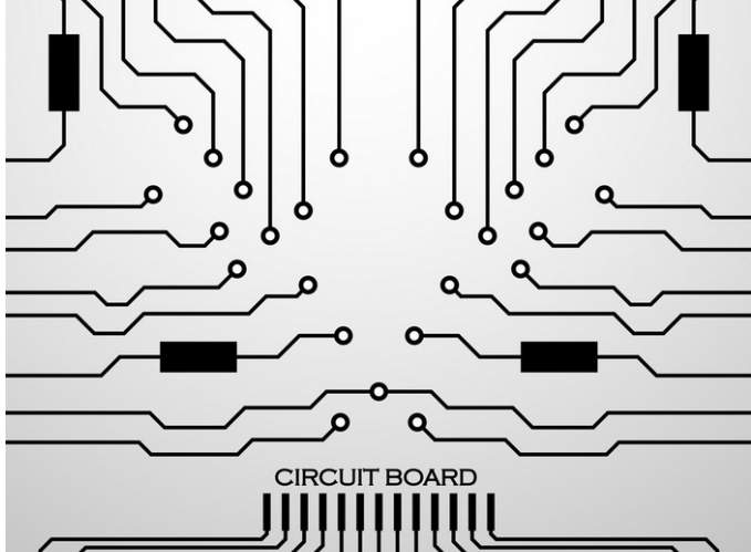
Circuit board schematic capture
Schematic capture can be used not only as a basis for designing electrical connections for circuit boards, but also as a legal document. Therefore, the schematic must be electrically correct, and it must also be readable and usable to other design team members, manufacturers, technicians, and end users. To accomplish all of this, here are the main steps you need to focus on when capturing a circuit board schematic.
Logical flow
When you lay out symbols and the networks they connect to, the logical flow and connections must be consistent and easy to understand. This is very important for high-speed circuits, where the PCB layout team needs to design the signal path according to the logical flow of the schematic.
Give yourself space
When placing symbols on the schematic, be sure to leave enough space for yourself. Not only will you need to draw a large number of networks from pin to pin, but these networks will also have names and pin numbers that need to be legible.
Don't be afraid to move symbols and networks around the schematic to make room. Your schematic capture system will be powerful for manipulating symbols and networks as well as cutting and pasting circuit areas. Make sure that all your reference codes, part numbers, values, and additional text are not overwritten by other schematic objects. Remember, the goal is to make readable and usable schematics, not to save paper.
Design rules and constraints
Although most design rules won't come into play until the design is ready for PCB layout, it's a good idea to create different network and component classes now. This will allow you to assign specific design constraints to the classes that you want your layout team to know and follow.
Characteristic
As you work, you may need to adjust certain properties in the schematic. Make sure you use the property editor to do this, as shown in the figure below. Here you use the property editor in Cadence's Allegro Design Entry CIS tool to adjust the value of the selected part.
Text information
In addition to the circuit, the schematic should contain basic information about the company and the board. This data will include the part number, product information, revision number, and company contact and copyright information.
Democratic Republic of Congo
The design rule check must be run in the schematic when designing the schematic, and then checked again before sending it to the PCB layout. This will prevent obvious errors, such as missing pin connections, all the way to manufacture.
Not only must the schematic be readable, but from a CAD tool point of view, it must also be usable. Creating a clean and organized schematic will help, and running design rule checks to ensure that the schematic database does not carry any errors in the layout. At this point, the schematic is almost ready to be laid out, but there are still a few things to do.
The properties editor that opens on the selected component
Simulation and PCB layout
Until now, the schematic capture process has focused on generating clean circuit board schematics without any connection errors. However, questions remain about how well these circuits are designed to perform. To find out, it is best to run the schematic through circuit simulation using SPICE tools of CAD systems. This will tell you whether your circuit will work as designed, predict the behavior of the board when it is running, and expose unexpected behavior in the circuit. SPICE tools also allow you to investigate different circuit design options without investing time and money in physical parts and people to build breadboards or prototypes.
Now that you are ready to turn the schematic into a layout, you need to prepare the design for the final step. This includes running final design rule checks and ensuring that all required properties, text, and circuit connections are correctly captured. After completing this preparation, you can create all the data files needed to transfer the board schematics to the layout and begin the PCB design phase.
Corrosion process of PCB circuit board
Feb 07,2023


Just upload Gerber files, BOM files and design files, and the KINGFORD team will provide a complete quotation within 24h.