
Professional PCB manufacturing and assembly
Building 6, Zone 3, Yuekang Road,Bao'an District, Shenzhen, China
+86-13410863085Mon.-Sat.08:00-20:00

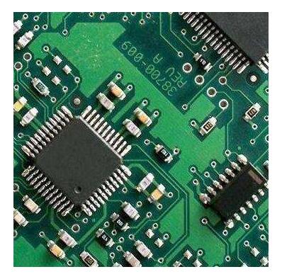
Through holes are also called metallized holes. In the double panel and multilayer plate, in order to connect the printed wires between the layers, a common hole is drilled at the junction of the wires that need to be connected in each layer, that is, through the hole. The parameters of the hole mainly include the outside diameter of the hole and the size of the hole.
One, through the hole model
From the effect of some PCB boards designed in the past, the influence of the hole on the low frequency and low speed signals is very small, but recently, with the increase of clock speed, the problem of the rise time of the device has become a key problem in PCB design. The influence of hole in PCB transmission line has become a hot topic of discussion.
1. Mathematical model of the hole
The through-hole model can also be considered as a parameter model composed of capacitance, inductance and resistance, just like a general transmission line. The through-hole model can be extracted by an extraction tool (such as ANSOFT), or tested by TDR test method.
In the simulation analysis of general simulation tools, the hole model is approximately replaced by 1pf capacitor. TDR test transient resistance drop is 6~7 ohms.
2. Influencing factors on the perforation model
It can be seen from the above formula that the main factors affecting the parameters of the hole are: the diameter of the hole, the thickness of the plate and the size of the hole pad. In addition, different layer Settings, where to change the layer through the hole, the impact of the plane layer are also influencing factors.
Second, the influence of the hole on signal conduction and radiation emission
1. Influence of aperture on impedance control
Note that the use of components that need to be drilled on the PCB board or the PCB that needs to be drilled through will cause discontinuity of the mirror plane, which will destroy the optimal return path of the signal.
For microstrip lines or strip lines that need to be perforated between different layers, there are fixed RF backflow routes around them, which are susceptible to interference. The easiest way to improve anti-interference performance is not to perforated wiring between different layers, only the same layer of wiring is the best, to ensure that there is no impedance discontinuity caused by any reason at any position of microstrip line and ground plane. If a sensitive signal line must be perforated, then the signal must be perforated near the hole to reduce the discontinuity.
Imagine that for wiring of more than four layers, there is a complete ground layer, a complete power layer, and other wiring layers. In order to ensure good signal return during wiring, the stratum should take the task of the main channel of return flow. If there are sensitive signals that need to be drilled through the hole and go to the adjacent layer of other non-stratum, then the signal line needs to be processed by wrapping. The ground wire should be parallel to the signal wire as close as possible.

The known negative effects of perforation can be roughly divided into the following categories:
(1) The hole is the inherent capacitance, so the characteristic impedance of PCB wiring is changed
(2) The perforation acts as a jump on the characteristic impedance of the line, thus resulting in reflection. The perforation leads to a transient impedance discontinuity of the line of 6-7 ohm, which leads to a negative reflection coefficient of about 0.055 (the characteristic impedance of the line of about 50 ohm), approximately 5%.
(3) When the routing changes from one layer to another layer, the reference plane will change, and the return path of the routing will also change. The characteristic impedance of the route may also vary greatly,
(4) If the line of a layer goes from this layer to another layer of the same reference level, the influence of the hole is small. Otherwise, the characteristic impedance of the transmission line may change greatly after the change of the reference plane.
Unfortunately, few studies have specifically examined the effect of holes on PCB routing without changing other parameters. This is due, at least in part, to the following resource constraints:
(1) A test PCB circuit board needs to be designed
(2) need to process
(3) A good tester is needed, and the researcher should be able to use it skillfully
2. Influence of the number of holes on signal quality
The effect of the number of holes on the signal needs to be verified. Virtually every hole (and even the line itself) has a slight high-frequency loss. According to the TDR test results, the hole does have a capacitative effect, which will lead to the attenuation of the signal's higher harmonics, which is manifested as the signal will slow down when rising.
However, in the case of a single hole, the resulting effect of the hole is negligible compared to the attenuation of the entire line. For a designer using a component (or faster) with a rise time profile of 0.5ns to 1.0s(500ps to 1000ps), the edge slowdown of tens of ps caused by a single pass hole is relatively insignificant. For very high speed designs, the effect of multiple pass holes should be considered and the number of pass holes should be minimized.
The hole will also cause the signal transmission to become longer, generally a hole affect about hundreds of ps wire delay. For long lines on the backplane: the effect of a hole is also negligible.
Suggestions on perforation in PCB design process:
(1) minimize the number of holes;
(2) When wiring is changed, the plane with continuous impedance is preferred for switching;
(3) For signals below 1GHZ, the inner wiring should be given priority to reduce the radiation impact, rather than avoid the hole.

Surface treatment technology
Feb 06,2023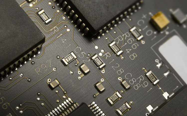


Just upload Gerber files, BOM files and design files, and the KINGFORD team will provide a complete quotation within 24h.