
Professional PCB manufacturing and assembly
Building 6, Zone 3, Yuekang Road,Bao'an District, Shenzhen, China
+86-13410863085Mon.-Sat.08:00-20:00


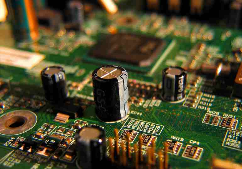
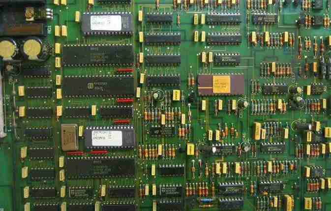
1. Some experience in reducing noise and electromagnetic interference.
(1) can use low-speed chips do not need high-speed chips, high-speed chips used in key places.
(2) Can be used to string a resistance method, reduce the control circuit up and down along the jump rate.
(3) Try to provide some form of damping for relays, etc.
(4) Use the lowest frequency clock that meets system requirements.
(5) Clock generator as close as possible to the device using the clock. The quartz crystal oscillator housing should be grounded
(6) Circle the clock area with the ground line and the clock line should be as short as possible.
(7)I/O drive circuit as close as possible to the edge of the printing board, so that it will leave the printing board as soon as possible. The signal entering the printed board should be filtered, the signal from the high noise area should also be filtered, and the series terminal resistance method is used to reduce the signal reflection.
(8) The useless end of MCD should be connected to the high, or grounded, or defined as the output end. The end of the integrated circuit should be connected to the power source, and do not hang.
(9) The input end of the idle gate circuit should not be suspended, the positive input end of the idle operational amplifier should be grounded, and the negative input end should be connected to the output end.
(10) Printed board as far as possible to use 45 line rather than 90 line wiring to reduce high-frequency signal transmission and coupling.
(11) The printed board is partitioned according to the frequency and current switching characteristics, and the noise element and the non-noise element should be further away.
(12) Single panel and double panel with single point power supply and single point grounding, power line, ground as thick as possible, economic is able to bear the use of multilayer board to reduce the power supply, ground inductive.
(13) Clock, bus, chip selection signal should be away from I/O lines and connectors.
(14) analog voltage input line, reference voltage end should be far away from the digital circuit signal line as far as possible, especially the clock.
(15) For class A/D devices, the digital part and the analog part would rather be unified rather than cross.
(16) The clock line perpendicular to the I/O line has less interference than the parallel I/O line, and the clock element pins are far away from the I/O cable.
(17) The pin of the component should be as short as possible, and the pin of the decoupling capacitor should be as short as possible.
(18) The key lines should be as thick as possible and protected on both sides. High-speed lines should be short and straight.
(19) The line sensitive to noise should not be parallel to the high-current, high-speed switching line.
(20) Do not run lines under quartz crystals and noise-sensitive devices.
(21) Weak signal circuit, low frequency circuit around do not form a current loop.
(22) Any signal should not form a loop. If it is unavoidable, make the loop area as small as possible.
(23) One decoupling capacitor for each integrated circuit. A small high-frequency bypass capacitor is added to the side of each electrolytic capacitor.
(24) Use large capacity tantalum capacitors or polycool capacitors instead of electrolytic capacitors as circuit charge and discharge storage capacitors. When using tubular capacitors, the case should be grounded.

2, good testability of mechanical contact conditions
Even circuits with very good electrical testability may be difficult to test without considering the basic rules of mechanics. Many factors can limit electrical testability. If the test points are insufficient or too small, it is difficult for the probe bed adapter to reach every node of the circuit. If the position error and size error of the test point are too large, it will cause the problem of poor test repeatability. A series of recommendations regarding the size and positioning of the latching holes and test points should be heeded when using the probe bed dispenser.
3. Electrical preconditions for optimum testability
Electrical preconditions are as important to good testability as mechanical contact conditions, and one cannot be without the other. A gate circuit cannot be tested either because it cannot reach the start input through the test point or because the start input is in the encapsulation shell and cannot be contacted externally. In principle, both cases are bad and make the test impossible. In the design of circuits, it should be noted that all components to be tested by on-line testing should have some mechanism that enables the individual components to be electrically insulated. This mechanism can be achieved by disabling the input, which can control the output of the component in a static high ohm state.
Although almost all test systems can drive the state of a node to any state by Backdriving, it is better to have a forbidden input for the node involved. First, bring the node to a high ohm state, and then "gently" add the corresponding level.
Similarly, the beat generator is always disconnected directly from behind the oscillator via a starter lead, gate circuit, or plug bridge. The starting input must never be connected directly to the circuit, but through a 100 ohm resistor. Each component should have its own start, reset, or control pin. It is necessary to avoid having many components whose startup inputs share a single resistance connected to the circuit. This rule applies to ASIC components, which should also have a lead pin through which the output can be brought to a high ohm state. If the element can be reset when the operating voltage is turned on, it is also very helpful to trigger the reset by the tester. In this case, the component can simply be placed in the specified state before testing.
Unused component pins should also be accessible, as undetected short circuits in these areas can also cause component failures. In addition, unused gate circuits are often used for design improvements later, and they may be converted into circuits. So it is also important that they are tested from the start to ensure that their artifacts are reliable.


Just upload Gerber files, BOM files and design files, and the KINGFORD team will provide a complete quotation within 24h.