
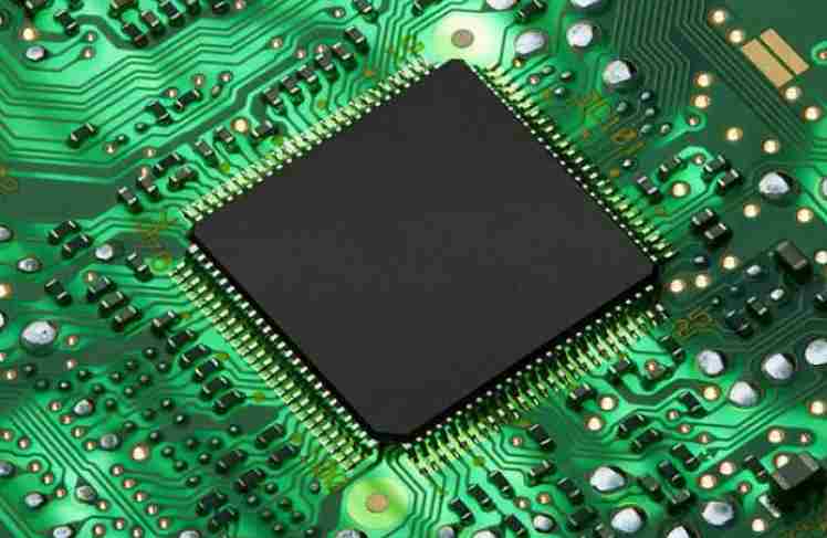
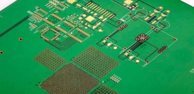
Professional PCB manufacturing and assembly
Building 6, Zone 3, Yuekang Road,Bao'an District, Shenzhen, China
+86-13410863085Mon.-Sat.08:00-20:00

With the advent of high-speed DSPS (digital signal processors) and peripherals, new product designers are faced with the increasing threat of electromagnetic interference (EMI). In the early days, the problem of emission and interference was called EMI or RFI (radio frequency interference). Now use the more definitive term "interference compatibility" instead. Electromagnetic compatibility (EMC) concerns both the emission and sensitivity of a system. If interference cannot be completely eliminated, it should be minimized. A DSP system is electromagnetic compatible if it meets the following three conditions.
1. It does not interfere with other systems.
2. Not sensitive to emission from other systems.
3. The system does not interfere.
Interference definition
Interference occurs when the energy of the interference causes the receiver to be in an undesirable state. Interference is generated either directly (through conductors, common impedance coupling, etc.) or indirectly (through crosstalk or radiation coupling). Electromagnetic interference is generated through conductors and through radiation. Many sources of electromagnetic emission, such as illumination, relays, DC motors and fluorescent lamps, can cause interference. AC power cables, interconnect cables, metal cables, and the internal circuitry of subsystems may also emit radiation or receive unwanted signals. In high speed digital circuits, the clock circuit is usually the largest source of broadband noise. In fast DSPS these circuits can produce harmonic distortion up to 300MHz and should be removed in the system. In digital circuit, the most easily affected are reset line, interrupt line and control line.
Conductive EMI
One of the most obvious and often overlooked paths that can cause noise in a circuit is through a conductor. A wire passing through a noisy environment picks up noise and sends it to another circuit to cause interference. The designer must avoid picking up the noise of the wire and remove the noise by decoupling method before the noise produces interference. The most common example is when noise enters a circuit through a power cord. If the power supply itself or other circuits connected to the power supply are interference sources, they must be decoupled before entering the circuit.
Common impedance coupling
Common-impedance coupling occurs when current from two different circuits flows through a common impedance. The voltage drop on the impedance is determined by two circuits. The ground current from the two circuits flows through the common ground impedance. The ground potential of circuit 1 is modulated by ground current 2. The noise signal or DC compensation is coupled from circuit 2 to circuit 1 via common ground impedance.
Radiation coupling
Coupling via radiation is commonly known as crosstalk. Crosstalk occurs when an electric current flows through a conductor to generate an electromagnetic field that induces a transient current in a neighboring conductor.
Radiation emission
There are two basic types of radiation emission: differential mode (DM) and common mode (CM). Common-mode radiation or monopole antenna radiation is caused by an unintentional voltage drop that elevates all ground connections in a circuit above the system ground potential. CM radiation is a more serious problem than DM radiation in terms of the size of the electric field. To minimize CM radiation, a practical design must be used to reduce the common-mode current to zero.
Factors that affect EMC
Voltage - Higher supply voltage means greater voltage amplitude and more emission, while lower supply voltage affects sensitivity.
Frequency - High frequencies generate more emission, periodic signals generate more emission. In high frequency digital systems, current spikes are generated when the device is switched on and off. In the simulation system, the current spike signal is generated when the load current changes.
Grounding - Nothing is more important to circuit design than a reliable and perfect power system. Among all EMC problems, the main problem is caused by improper grounding. There are three signal grounding methods: single point, multipoint, and hybrid. The single point grounding method can be used at frequencies below 1MHz, but is not suitable for high frequencies. In high frequency applications, multipoint grounding is preferable. Hybrid grounding is a method of single-point grounding for low frequency and multipoint grounding for high frequency. The ground layout is critical. A high frequency digital circuit and a low level analog circuit must not mix ground circuits.
PCB design - Proper printed circuit board (PCB) wiring is essential to prevent EMI.
Power decoupling - When the device is switched on and off, transient currents are generated in the power line and must be attenuated and filtered out. The transient currents from high di/dt sources cause ground and trace "emission" voltages. High di/dt generates a wide range of high frequency current, which excites components and cable radiation. Changes in current and inductance flowing through the wire cause a voltage drop, which is minimized by reducing the change in inductance or current over time.
Noise reduction techniques
There are three ways to prevent interference:
1. Suppress source emission.
2. Make the coupling path as invalid as possible.
3. Minimize the sensitivity of the receiver to transmission.
The following describes the board level noise reduction technology. Board level noise reduction technology includes board structure, line arrangement and filtering.
Panel structure noise reduction technology includes:
* Use ground and power panels
* The plate area should be large to provide low impedance for power decoupling
* Keep surface conductors to a minimum
Use narrow lines (4 to 8 mil) to increase high frequency damping and reduce capacitive coupling
* Separate digital, analog, receiver, transmitter ground/power lines
* Separate the circuits on the PCB by frequency and type
* Do not cut PCB marks, stitches near the marks may cause unwanted loops
* Use multilayer panels to seal the thread between the power supply and the floor layer
* Avoid large open-loop laminate structures
* The PCB connector is connected to the housing, which provides shielding against radiation at the circuit boundary
* Low impedance of high frequency ground with multi-point grounding
* Keep the ground pin shorter than 1/20 of the wave length to prevent radiation and ensure low impedance line arrangement noise reduction techniques include using 45. Not 90. Stitch steering, 90. Steering increases capacitance and causes a change in the characteristic impedance of the transmission line
* Keep the spacing between adjacent excitation tracks larger than the width of the tracks to minimize crosstalk
* The clock signal loop area should be as small as possible
* High-speed lines and clock signal lines should be short and directly connected
* Sensitive wires should not be parallel to wires transmitting high current fast switching signals
* Do not have empty digital input to prevent unnecessary switching and noise generation
* Avoid supply lines under crystal oscillators and other inherent noise circuits
* The corresponding power supply, ground, signal and return track should be parallel to eliminate noise
* Keep clock lines, buses, and chips enabled separate from input/output lines and connectors
* Route clock signal orthogonal I/O signal
* To minimize crosstalk, the trace is crossed and scattered with the ground line at right angles
* Protect key track (4 mil-8 mil-track to minimize inductance, path close to floor layer, sandwich structure between plates, protect each side of the sandwich)
Filtering techniques include:
* Filter the power cord and all incoming signals to the PCB
* High frequency low inductance ceramic capacitors (0.1UF for 14MHz, 0.01UF for more than 15MHz) are used to decouple the primary pin at each point of the IC
* Bypass analog circuits for all power supply and reference voltage pins
* Bypass fast switching device
* Power/Ground decoupling at the device lead
* Multistage filtering is used to attenuate multi-frequency power supply noise

Other noise reduction design techniques are:
* Install the crystal oscillator into the plate and ground it
* Mask where appropriate
* Use series terminals to minimize resonance and transmission reflection. Impedance mismatches between load and line can result in partial reflection of the signal. Reflections include instantaneous perturbations and overshoot, which can generate large EMI
* Arrange the adjacent ground wire close to the signal wire to prevent the occurrence of electric field more effectively
* Placing the decoupled driver and receiver appropriately close to the actual I/O interface reduces coupling to the rest of the PCB and reduces radiation and sensitivity
* Shielding and stranding of interfered leads to eliminate mutual coupling on PCB
* Clamp diode on inductive load
EMC is an important problem to be considered in DSP system design. Appropriate noise reduction technology should be adopted to make DSP system conform to EMC requirements
Reliability design of printed circuit board
Feb 06,2023


Just upload Gerber files, BOM files and design files, and the KINGFORD team will provide a complete quotation within 24h.