
Professional PCB manufacturing and assembly
Building 6, Zone 3, Yuekang Road,Bao'an District, Shenzhen, China
+86-13410863085Mon.-Sat.08:00-20:00

The interconnection of circuit board system includes three types: chip to circuit board, PCB interconnect and PCB interconnect with external components. In RF design, the electromagnetic characteristics at the interconnect point is one of the main problems in engineering design. This paper introduces various techniques of the three types of interconnect design, including device installation methods, wiring isolation and measures to reduce lead inductance.
There are signs that PCB design is becoming more frequent. As data rates continue to increase, the bandwidth required to transmit data pushes the signal frequency limit up to 1GHz and beyond. This high frequency signal technology is far beyond the millimeter wave (30GHz) range, but it does involve RF and low end microwave technology.
RF engineering design methods must be able to deal with the strong electromagnetic field effects normally generated at higher frequency bands. These electromagnetic fields can induce signals on adjacent signal lines or PCB lines, causing nuisance crosstalk (interference and total noise) and impairing system performance. Backloss is mainly caused by impedance mismatch, which has the same effect on the signal as additive noise and interference.
High loop loss has two negative effects: 1. The signal reflected back to the signal source will increase the system noise, making it more difficult for the receiver to distinguish the noise from the signal; 2. 2. Any reflected signal basically degrades the signal quality because the shape of the input signal changes.
Although the digital system only handles 1 and 0 signals and is very fault-tolerant, the harmonics generated when the high speed pulse rises cause the signal to become weaker at higher frequencies. Although forward error correction can eliminate some of the negative effects, part of the bandwidth of the system is used to transmit redundant data, resulting in reduced system performance. A better solution is to let RF effects help rather than hurt signal integrity. The recommended total recovery value at the highest frequency of the digital system (usually the differential data point) is -25dB, which corresponds to a VSWR of 1.1.
PCBS are designed to be smaller, faster and less costly. For RF PCBS, high-speed signals sometimes limit the miniaturization of PCB designs. At present, the main way to solve the crosstalk problem is to manage the ground layer, spacing the wiring and lowering the lead capacitance. The main method to reduce the loss is impedance matching. This method includes the effective management of insulation materials and the isolation of active signal lines and ground lines, especially between the signal lines and ground where the state changes.
As the interconnection point is the weakest link in the circuit chain, the electromagnetic property of the interconnection point is the main problem facing the engineering design in RF design. It is necessary to investigate each interconnection point and solve the existing problems. Circuit board system interconnection includes chip to circuit board, PCB board interconnection and signal input/output between PCB and external devices.
1. Interconnection between chip and PCB board
The Pentium IV and high-speed chips with a large number of input/output interconnects are already available. As for the chip itself, its performance is reliable, and the processing speed has been able to reach 1GHz. The most exciting thing about the recent GHz interconnection symposium (www.az.ww.com) was that the approach to dealing with the increasing volume and frequency of I/O is already well known. The main problem of chip and PCB interconnection is that the high interconnection density will cause the basic structure of PCB material to become a factor limiting the increase of interconnection density. One innovative solution presented at the conference is to use a local wireless transmitter inside the chip to transmit data to a nearby circuit board.
Whether or not this solution works, it was clear to the participants that IC design technology is far ahead of PCB design technology in terms of high frequency applications.
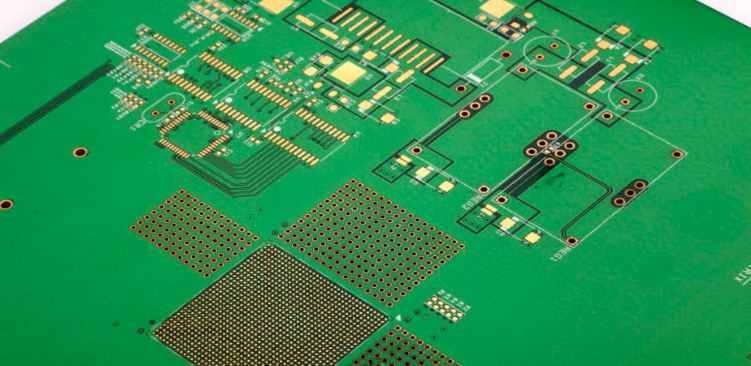
Two, PCB board interconnection
The tips and methods for high frequency PCB design are as follows:
1. The corner of the transmission line should adopt a 45° Angle to reduce back loss (Figure 1);
2. To use insulation constant value according to the level of strict control of high performance insulated circuit board. This method is beneficial to effectively manage the electromagnetic field between insulation material and adjacent wiring.
3. PCB design specifications for high precision etching should be perfected. Consider again specifying a total error of line width of +/-0.0007 inches, managing undercut and undercut of a wiring shape and specifying siding conditions. The overall management of wiring (wire) geometry and coating surfaces is important to the solution of skin effects related to microwave frequencies and to the implementation of these specifications.
4. Protruding leads exist tap inductance, to avoid the use of lead components. At high frequencies, surface mounted components are preferred.
5. For signal through holes, avoid using through hole machining (pth) process on sensitive plates, as this process will cause lead inductance at the through holes. Lead inductance can affect layers 4 to 19 if a single through hole in a 20-layer board is used to connect layers 1 to 3.
6. Provide abundant ground connections. Molded holes should be used to connect these connections to prevent the influence of 3 - dimensional electromagnetic fields on the circuit board.
7. To choose non-electrolytic nickel plating or dipping process, do not use HASL method for plating. This electroplated surface provides a better skin effect for high frequency currents (Figure 2). In addition, this highly weldable coating requires fewer leads, helping to reduce environmental pollution.
8. Solder resistance layer can prevent the flow of solder paste. However, due to the uncertainty of thickness and the unknown insulation properties, the entire surface of the plate covered with solder resistance material will lead to a large change in the electromagnetic energy of the microstrip design. Generally use solder dam as solder layer.

If you are not familiar with these methods, consult an experienced design engineer who has worked on microwave circuit boards for the military. You may also want to discuss with them the price range you can afford. For example, it is more economical to use copper-backed coplanar microstrip designs than strip-line designs. You can discuss this with them to get better advice. Good engineers may not be used to thinking about cost, but the advice can be quite helpful. Now we should try our best to train those young engineers who are not familiar with RF effect and lack of experience in dealing with RF effect. This will be a long-term work.
In addition, other solutions can be used, such as improved computing models with RF effect processing capabilities.
Noise reduction technology of DSP system
Feb 06,2023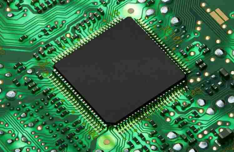


Just upload Gerber files, BOM files and design files, and the KINGFORD team will provide a complete quotation within 24h.