
Professional PCB manufacturing and assembly
Building 6, Zone 3, Yuekang Road,Bao'an District, Shenzhen, China
+86-13410863085Mon.-Sat.08:00-20:00

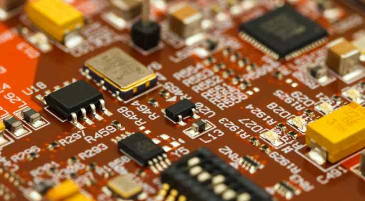
Whether in PCBA patch processing or PCBA proofing, if you want to reduce the loss of components, so that your production cost is lower, better quality, then you need to follow certain operating rules, only master the correct operation method and these rules can make the product better, lower cost. What are the operating rules of PCBA proofing?
Operating rules of PCBA proofing:
1. In the PCBA working area, there shall be no food or drink, no smoking, no sundry things unrelated to work, and the workbench shall be kept clean and tidy.
2. The welded surface in PCBA proofing shall not be taken with bare hands or fingers, because the grease secreted by human hands will reduce the weldability and prone to welding defects.
3. Reduce the operation steps of PCBA and components to a minimum to prevent danger. In assembly areas where gloves must be used, soiled gloves can cause contamination, so replace gloves as often as necessary.
4. Do not use skin-protecting oils on your hands or any detergent containing silicone, which can cause problems with solderability and adhesive properties of the coating. Specially formulated detergents for PCBA welding surfaces are available.
5. EOS/ESD sensitive components and PCbas must be identified with appropriate EOS/ESD logo to avoid confusion with other components. In addition, in order to prevent ESD and EOS from endangering sensitive components, all operation, assembly and testing must be completed on the workbench which can control static electricity.
6. Check the EOS/ESD workbench periodically to ensure that they work properly (anti-static). Various hazards of EOS/ESD components can be caused by incorrect grounding methods or oxides in the ground connection, so special protection should be given to the "third wire" ground terminal connector.
7. It is forbidden to stack PCBA, which will cause physical damage. Special brackets of various kinds should be configured on the assembly working face, and they should be placed according to types.

What are the effects of voids on patch processing? In the series of articles analyzing the reasons for welding quality in the process of patch processing, we have made a certain analysis of the reasons for the voids caused by pcb coating in the process of patch processing. Today, Baiqiancheng Electronics is looking for the starting point of problems caused by voids, starting from the SMT patch processing process itself. First:
(1) Melting point of BGA welding ball and solder paste: For BGA solder joint, if the melting point of the welding ball is lower than the melting point of the solder paste, a void may occur. Since the solder ball melts and covers the solder paste first, it is easy to capture the flux.
(2) solder paste printing thickness: the thicker the solder paste printing thickness, the less the gap. Because thicker solder paste has a greater ability to remove oxides from the flux, this helps air bubbles escape.
(3) Temperature curve: Considering the reduction of gas volatilization, the use of long-term high temperature preheating and short-term low peak temperature is conducive to reducing cavitation.
smt processing
It should be noted that the long term high temperature preheating and short term low temperature peak temperature requirements are opposite to the commonly recommended temperature curve requirements. In fact, it's a combination. Long-term peak temperature at high temperature is beneficial to the performance and wetting of the flux and can greatly reduce the possibility of ball and socket phenomenon.
(4) Welding pressure: We know that when welding under vacuum condition, there is almost no cavity in the weld. Not that volatiles are not produced, but that there are fewer bubbles (less oxidation) and that they are easy to escape. The use of N 2 gas, although the continuous oxidation of the heating process is reduced, but the air pressure in the furnace is higher, and bubbles do not easily escape, so the voids are usually larger.
Now the rapid development of the electronic processing industry, mobile phones, computers, household appliances and other products in the continuous upgrading and iteration, the current products may be in the tuyere, but this tuyere may be fleeting. Therefore, there is not much time for trial and error in the production of a product, so the best way is to select one or several factories for PCBA proofing after the design is completed and before the formal production.
Some people may ask at this time why do you want to do so, what is the purpose of doing so? The following Shenzhen hundred thousand into electronic small make up to talk about the reasons for PCBA proofing.
Usually, before mass production, a factory or several factories will be selected for PCBA proofing. There are usually two purposes for doing this:
First: check whether there is any problem with the design process of PCBA and whether there is anything that needs to be modified.
Second: Select competent factories, which can ensure the finished product rate and test pass rate of PCBA production, have an assessment of the general delivery time and quality, and have an accurate estimation of various situations of mass orders in the later stage. You can check our company's online webcast to see the factory
Why choose PCBA to contract labor and materials?
Currently, there are generally two kinds of processing methods in electronic manufacturing, namely, processing with supplied materials and processing with contracted work. Processing with supplied materials means that the customer provides the materials, while the factory provides SMT patch processing and DIP plug-in processing, etc., while processing with contracted work means that the customer provides a full set of materials, and the factory is responsible for purchasing and production. Faced with these two production and processing methods, There are more and more customers choose the latter - labor package material, this is why?
More and more people choose PCBA to contract work and materials mainly for the following reasons:
First, let professional people do professional things
The electronic manufacturing factory has a perfect department system, a clear division of labor, rich experience, and many ways of procurement, so that the handled links are streamlined to a minimum, which is helpful to shorten the delivery time.
Two, cost savings
SMT SMT of Shenzhen Baiqiancheng Electronics: The processing method of contracted labor and materials can make the customer's labor cost, time cost, material cost greatly reduced.


Just upload Gerber files, BOM files and design files, and the KINGFORD team will provide a complete quotation within 24h.