
Professional PCB manufacturing and assembly
Building 6, Zone 3, Yuekang Road,Bao'an District, Shenzhen, China
+86-13410863085Mon.-Sat.08:00-20:00

Share the specific process of PCBA proofing: Now many customers will give their products to professional processing manufacturers for production, and then generally carry out PCBA proofing before mass production. Then what is the proofing process of PCBA? The following is a detailed introduction to you by the hundred thousand small series.
First, customer orders. Customers will according to their actual needs to their own trusted electronic processing plant orders, and put forward specific requirements. The processing plant will evaluate its capacity to see if it can fulfill the order. If the manufacturer is sure that they can complete the order within a certain time, then the two parties will negotiate to determine the production details.
Second, customer data. After the customer decides to place an order, he will provide a series of documents and lists to the electronics processing plant, such as PCB electronic files, coordinate files, BOM list and so on, which must be provided.
Third, purchase raw materials. Electronic processing plant according to the documents provided by the customer to the designated supplier to purchase the relevant raw materials.
Fourth, incoming material inspection. Before PCBA proofing, the electronic processing plant needs to carry out strict quality inspection for all the raw materials to be used, and can only be put into production after ensuring that they are qualified.
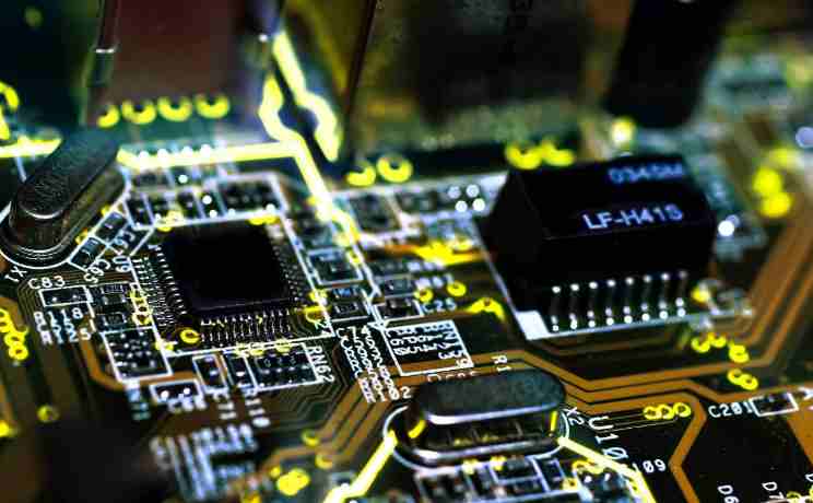
Fifth, PCBA production. In the PCBA proofing, in order to ensure the production quality, whether it is patch or welding production, the manufacturer needs to strictly control the furnace temperature.
Sixth, PCBA test. Electronics manufacturers also need to carry out rigorous testing, only passing the test PCB board can be delivered to the customer.

Seventh, packaging after sale. After the PCBA proofing is completed, the product needs to be packaged and then handed over to the customer to complete the whole proofing work.
smt rapid proofing factory's PCBA proofing proofing notes:
1, the welding surface cleaning must use professional configuration of cleaning agent.
2, after smt rapid proofing of the circuit board can not be stacked, otherwise it will cause physical damage to the board.
3. EOS/ESD sensitive components and PCbas shall be marked with appropriate EOS/ESD labels.
4, maintain the operation table cleaning and clean. All kinds of food and drinks are not allowed in the working area. Smoking, cigarette rolls and ashtrays are strictly prohibited.
5. Reduce the operation process of components to the minimum limit to prevent risks.
6. The welded surface of the circuit board cannot contact the human skin directly, otherwise the grease will affect the reliability of welding.
The above is the "PCBA proofing processing process and processing matters to be noted" to share, processing components to remember to be careful, pay attention to prevent bad things. At the same time, we also need to carry out a strict test on our processed products to ensure that the quality of the products reaches the customers.
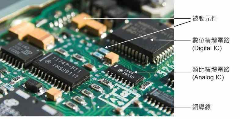
As we all know, the technology of patch processing is more and more advanced, which also indicates that we will go to a higher level in the field of patch processing. Do you know that in the patch processing industry, the processed patch should be packaged? And there are many kinds of packaging technologies, such as: BGA(ball grid array), ceramic (C- ceramic) means ceramic packaging, COB(chip on board) chip packaging, DIP(dual in-line package), DIP is the most popular plug-in package. DIC(dual in-line ceramic package) DIP and so on. These packaging techniques are advanced, but why is BGA patch packaging more common and more effective? The following achievements in detail we explain the advantages of BGA patch packaging.
1, BGA package in addition to the chip itself, some interconnection lines, very thin substrate, and plastic cover, there is nothing else, few exposed components outside. No big pins, no lead out box. The entire chip can be as high as 1.2 mm on the PCB, which is one of the biggest advantages of the BGA package.
2. The pins of the BGA package look cool and neatly arranged at the bottom. This method has a very big advantage that it is conducive to the repair of the BGA chip, because it is easy to find the damaged position to remove according to its alignment.
3, the signal from the chip, through the connection line matrix, then to your PCB, and then through the power/ground pins back to the chip to form a total loop. Less stuff around the perimeter, smaller size means smaller overall loop. With the same number of pins, the size of the BGA package loop is usually 1/2 to 1/3 that of the QFP or SOIC. A smaller loop means less radiation noise and less crosstalk between pins.
4. BGA packaging can also efficiently design the distribution of power supply and ground pins, because the existence of ground elastic effect also makes the number of power supply and ground pins continuously reduced.
5. The BGA package is very strong. Compared with the 20mil pitch QFP, the BGA has no pins that can be bent and broken. It is as solid as brick. Generally, if you want to remove the BGA package, you must use the BGA repair table to remove at high temperature.
6, BGA package can put a lot of power and ground pins in the middle, I/O port leads on the periphery. This is simply a method that can be used to pre-wire the BGA substrate to avoid confusing I/O port routing.
7, advanced BGA package, can put all the pins right under the chip, will not exceed the chip package, which is very good for miniaturization.
8, BGA packaging has a relatively big advantage is that the pad is relatively larger, easy to operate in the operation of repair. It is much larger than the inverted crystal packaging method, which requires the pad to be placed directly on the silicon wafer. The pad needs to be smaller, which can cause some problems and manufacturing problems. Chamferous packaging technology is to some extent invisible mystery, in fact, is not worthy of the name. This problem can be solved through the BGA process.
9. No more advanced PCB process is required. It does not need to consider the matching heat transfer efficiency of chip and PCB size to prevent silicon chip damage as C4 and direct inverted crystal packaging. The BGA package connection matrix has an adequate mechanism to ensure heat pressure on the silicon wafer. No mismatches, no difficulties.
10, a small package itself, has good heat dissipation attributes. If the silicon wafer is attached to it, most of the heat can be transferred down to the ball array of the BGA. If the silicon wafer is attached to the underside, then the back of the silicon wafer is connected to the top of the package, which is a reasonable way to dissipate heat.
What are the operating rules of PCBA proofing?
Feb 04,2023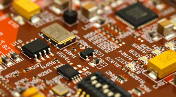


Just upload Gerber files, BOM files and design files, and the KINGFORD team will provide a complete quotation within 24h.