
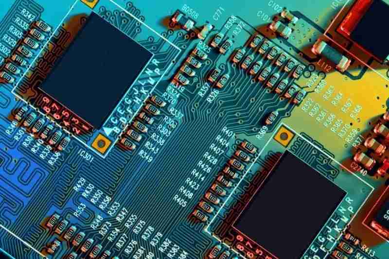
Professional PCB manufacturing and assembly
Building 6, Zone 3, Yuekang Road,Bao'an District, Shenzhen, China
+86-13410863085Mon.-Sat.08:00-20:00


1. Raising SI problems
As the speed of IC output switches increases, almost all designs encounter signal integrity problems regardless of signal cycle. Even if you haven't had SI problems in the past, you're bound to have signal integrity problems in the future as the frequency of the circuit increases.
The signal integrity problem mainly refers to the signal overshoot and damping oscillation, which are mainly functions of IC drive amplitude and jump time. That is, even if the wiring topology does not change, as long as the chip speed becomes fast enough, the existing design will go critical or stop working. We use two examples to illustrate that signal integrity design is inevitable.
In communications, leading telecom companies are producing high-speed circuit boards (above 500MHz) for voice and data interchange, where cost is not particularly important and where multilayer boards can be used. The circuit board can be sufficiently grounded and easily formed into a power supply circuit. A large number of discrete terminals can also be used as required, but the design must be correct and not in a critical state.
SI and EMC experts perform simulations and calculations before wiring, and then the citical board design can follow a very strict set of design rules, and where in doubt, terminating devices can be added to gain as much SI safety margin as possible. In the actual working process of the circuit board, there will always be some problems, so the SI problem can be avoided by using the controlled impedance terminal connection. In short, superstandard design can solve SI problems.
The following introduces the general SI design criteria for the design process.
2. Preparation before design
Before the design begins, it is necessary to think and determine the design strategy, so as to guide the selection of components, process selection and cost control of circuit board production. In the case of SI, research should be conducted in advance to form planning or design guidelines to ensure that the design results do not have obvious SI problems, crosstalk or timing issues. Some design guidelines can be provided by IC manufacturers, however, chip vendor guidelines (or your own design guidelines) have limitations that may not allow you to design a board that meets SI requirements. If design rules were easy, there would be no need for design engineers.
Before you can actually wire the circuit, you need to solve the following problems, which in most cases will affect the circuit board you are designing (or are considering designing), and this work is worthwhile if the number of circuit boards is large.

3. Layering of circuit boards
Some project teams have a lot of discretion in how many PCB layers to set, while others don't, so it's important to know where you stand. Communication with the manufacturing and cost analysis engineers can determine the stack error of the board, and this is an opportunity to discover the board manufacturing tolerances. For example, if you specify that a certain layer is 50Ω impedance control, how does the manufacturer measure and ensure this value?
Other important questions include: What are the expected manufacturing tolerances? What is the expected insulation constant on the board? What is the allowable error in line width and spacing? What is the allowable error for the thickness and spacing of the grounding and signal layers? All of this information can be used during the pre-wiring phase.
Based on the above data, you can choose to cascade. Note that almost every PCB inserted into another board or backboard has a thickness requirement, and most board manufacturers have fixed thickness requirements for the different types of layers they can make, which will greatly constrain the final number of layers. You may want to work closely with the manufacturer to define cascading numbers. Impedance control tools should be used to generate target impedance ranges for the different layers, making sure to take into account manufacturer-supplied allowable manufacturing errors and the effect of adjacent wiring.
Ideally, when the signal is intact, all high-speed nodes should be routed inside the impedance control layer (such as ribbon lines), but in practice, engineers must often use the outer layer to route all or part of the high-speed nodes. To optimise the SI and keep the boards decoupled, the grounding/power layers should be arranged in pairs whenever possible. If you can only have one docking layer/power layer, you'll have to make do. If there is no power layer at all, by definition you may run into SI problems. You may also run into situations where it is difficult to emulate or emulate the performance of the board without defining the return path of the signal.
4. Crosstalk and impedance control
Coupling from adjacent signal lines causes crosstalk and changes the impedance of the signal line. Coupling analysis of adjacent parallel signal lines may determine the "safe" or expected spacing (or length of parallel wiring) between signal lines or between various types of signal lines. For example, if you want to limit the crosstalk from the clock to the data signal node to 100mV, but keep the signal lines parallel, you can find, by calculation or simulation, the minimum allowable distance between the signals on any given wiring layer. Also, if the design includes impedance critical nodes (either clocks or dedicated high-speed memory architectures), you must place the wiring on one (or several) layers to get the desired impedance
5. Important high-speed nodes
Delay and time delay are the key factors that must be considered in clock routing. Because of the strict timing requirements, such nodes usually have to be terminated to achieve the best SI quality. These nodes are identified in advance and the time required to place and wire the regulating elements is planned to adjust the pointer to the signal integrity design.
6. Technology selection
Different driving techniques are suitable for different tasks. Is the signal point-to-point or point-to-multiple taps? Is the signal coming out of the circuit board or staying on the same circuit board? What is the allowable time delay and noise margin? As a general criterion for signal integrity design, the slower the conversion speed, the better the signal integrity. There is no reason for a 50MHZ clock to have a 500PS rise time. A 2-3NS swing rate control device should be fast enough to ensure SI quality and help solve problems such as output synchronous switching (SSO) and electromagnetic compatibility (EMC).
The advantage of driver technology can be found in new FPGA programmable technology or user-defined ASics. With these custom (or semi-custom) devices, you have a wide range of options for driving range and speed. Early in the design process, meet FPGA(or ASIC) design time requirements and determine appropriate output choices, including pin selection if possible.
In this design phase, appropriate simulation models should be obtained from IC suppliers. In order to effectively cover the SI emulation, you will need an SI emulation program and the corresponding emulation model (possibly the IBIS model).
Finally, you should establish a series of design guidelines during the pre-wiring and wiring phases, which include: target layer impedance, wiring spacing, preferred device processes, critical node topology, and terminal planning.

7、Pre-wiring phase
The basic process of pre-wiring SI planning is to first define input parameter ranges (drive amplitude, impedance, tracking speed) and possible topological ranges (minimum/maximum length, short line length, etc.), then run each possible simulation combination, analyze timing and SI simulation results, and finally find an acceptable numerical range.
Next, the working range is interpreted as the wiring constraints of PCB wiring. Different software tools can be used to perform this type of "sweep" preparation, and the wiring program automatically handles such wiring constraints. For most users, timing information is actually more important than SI results, and the results of interconnection simulation can change the wiring to adjust the timing of the signal path.
In other applications, this process can be used to determine the layout of pins or devices that are incompatible with system timing Pointers. At this point, it is possible to fully determine which nodes need to be wired manually or which do not need to be terminated. For programmable devices and ASics, the choice of output drivers can also be adjusted at this time to improve the SI design or avoid discrete terminating devices.
8. SI simulation after wiring
In general, it is difficult for SI design guidelines to ensure that no SI or timing problems will occur after the actual wiring is completed. Even if the design is guided by guidelines, unless you can continuously check the design automatically, there is no guarantee that the design will fully comply with the guidelines, and problems will inevitably arise. Post-wiring SI emulation checks will allow design rules to be systematically broken (or changed), but only as necessary for cost reasons or strict wiring requirements.
9. Post-manufacturing stage
The above measures can ensure the SI design quality of the circuit board. After the circuit board assembly is completed, it is still necessary to put the PCB circuit board on the test platform, measure it with oscilloscope or TDR(time domain reflectometer), and compare the real circuit board with the simulation expected results. These measurements can help you improve the model and manufacturing parameters so that you can make better (and less constrained) decisions on your next pre-design survey.
10. Model selection
Much has been written about model selection, and engineers doing static timing validation may have noticed that, despite all the data available from device data sheets, it is still difficult to build a model. SI simulation model is on the contrary, it is easy to build the model, but it is difficult to obtain the model data. In essence, the only reliable source of SI model data is the IC vendor, who must work in tacit coordination with the design engineer. The IBIS model standard provides a consistent data carrier, but the cost of building the IBIS model and ensuring its quality is high. IC vendors still need to invest in it to be demand-driven, and circuit board manufacturers may be the only demand-side market.


Just upload Gerber files, BOM files and design files, and the KINGFORD team will provide a complete quotation within 24h.