
Professional PCB manufacturing and assembly
Building 6, Zone 3, Yuekang Road,Bao'an District, Shenzhen, China
+86-13410863085Mon.-Sat.08:00-20:00

pcb proofing is a must for the future production, because a lot of things need to be tested before mass production, otherwise there will be large-scale waste, but there are a lot of things to pay attention to in the early stage of proofing, otherwise it will need to waste a lot of things over and over again.
1. Physical boundary production
The closed physical framework is the basic platform for component layout and PCB proofing in the future. Must be very need to pay attention to the accuracy, but also to prevent being scratched, to pay attention to safety, protect themselves, this is a very key issue.
2. Introduce components and networks and lay out components
When pcb proofing , pull components and network into the pull frame, be sure to follow the prompts carefully, including the packaging form of components and network problems of components. Because of the contrast, so easy to go wrong. During PCB proofing, the layout of components and wiring has great influence on product life, stability and electromagnetic compatibility, so special attention should be paid to it. It also has something in principle, so pay special attention to this category as well.
3. PCB design, wiring and adjustment improvement
When designing and wiring PCB, pay attention to the requirements of processing parameters, or find a reliable PCB proofing manufacturer, the defective rate will be greatly reduced. After the completion of PCB design and wiring, only need to make some adjustments to the text, individual components, wiring and copper coating design and wiring, but also for the convenience of production, debugging and maintenance. So it's critical that we get an overall overhaul.
4. Check the cable
Sometimes due to commiseration or negligence, the network relationship of the drawn PCB board is different from the schematic diagram. This is where the checks come in. Therefore, after drawing should be checked first, and then the follow-up work. So you have to be careful in this area or you're going to have a lot of sex, which is really bad.

So there are a lot of problems that need to be noticed in the early work, otherwise there will be a large amount of things wasted to this is very undesirable, so of course, we should also find a reliable manufacturer to make, which is also very conducive to this aspect.
The significance of high frequency board
The increasing complexity of circuit board electronic components requires faster signal flow rates and therefore higher transmission frequencies, as well as high-frequency techniques to look at the width of the conductor used as an electronic component due to the short rise time of the pulse in the electronic component.
The signals of the high frequency board are reflected on the board, which means that the impedance varies according to the sending component. To prevent this capacities effect, all factors of the HF board must be accurately specified and controlled at the highest level of process. For high frequency board, it is critical to impedance in high frequency board conductor trace geometry, layer construction and dielectric constant of the material used. On high-frequency board boards, such as for wireless applications and data rates in the higher GHz range, there are special requirements for the materials used in high-frequency board boards, such as suitable dielectric constant, low attenuation, efficient transmission signal, homogeneous structure with low insulation thickness and dielectric constant tolerance, etc.
For many HF board applications, the use of FR4 materials is achieved with an appropriate layer accumulation, and the improved dielectric properties of the HF materials can be treated with HF equipment. They have a very low loss factor, low dielectric constant, and are primarily temperature - and frequency-independent. Other beneficial properties of HF boards are high glass transition temperature, excellent thermal durability and very low hydrophilic.
Concept of pcb proofing

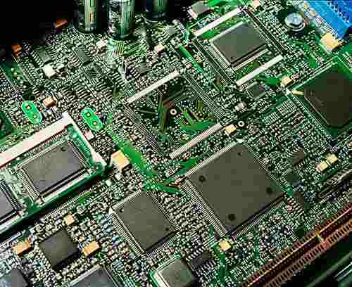
When it comes to PCB, I believe that most people are relatively unfamiliar. pcb refers to printed circuit board, also known as printed circuit board and printed circuit. It is an important electronic component, also the support body of electronic components, or the supplier of electrical connection of electronic components. Because PCB is made of electronic printing, so it is also known as printed circuit board. So what is pcb proofing? Let's explore pcb proofing together!

PCB proofing refers to the trial production of printed circuit boards before mass production. Its main function is the process of small batch trial production to the factory after the electronic engineers have designed the circuit and completed the PCB. However, there is usually no specific standard for the production quantity of PCB trial production. In general production, it is called pcb proofing before the completion of product design confirmation and testing.
PCB production process is varied, such as printed circuit board, pressing, text printing, making inner line, contact processing, drilling, welding proof green paint, plating through hole primary copper, outer line secondary copper, molding cutting and final inspection packaging. So what should we pay attention to when PCB proofing? As follows:
① We should pay attention to the quantity of proofing, which can effectively control the cost.
② Confirm device packaging to prevent proofing failure due to packaging errors.
(3) A comprehensive electrical inspection is needed to improve the electrical performance of PCB board.
(4) A good signal integrity layout can reduce noise and improve the stability of PCB.
Then do you have any good pcb proofing manufacturers recommend? KBIDM (Creation Factory) is very excellent, with scientific innovation service, inspection service, BOM service, scheme design, high-speed PCB design, PCB manufacturing, PCBA assembly and other services. The strength of the Creation Factory is the integration of innovative design and manufacturing services such as high-speed PCB design, IDH services and EES electronic engineering services.
Can provide customers with the full plate, core board, bottom plate personalized customization, quickly realize the product, R & D personnel of the whole process connection, to ensure that every detail is impeccable.
We have excellent production equipment, such as impedance detector, AOI system (automatic optical detection machine), secondary automatic copper plating line, machine line body, X-ray drilling machine, ore-treatment area universe horizontal line, short line, newly installed patch machine YG12 and other equipment. Only with good technology and production equipment to produce good performance of PCB.

How to choose Pcba manufacturer?
Jan 15,2023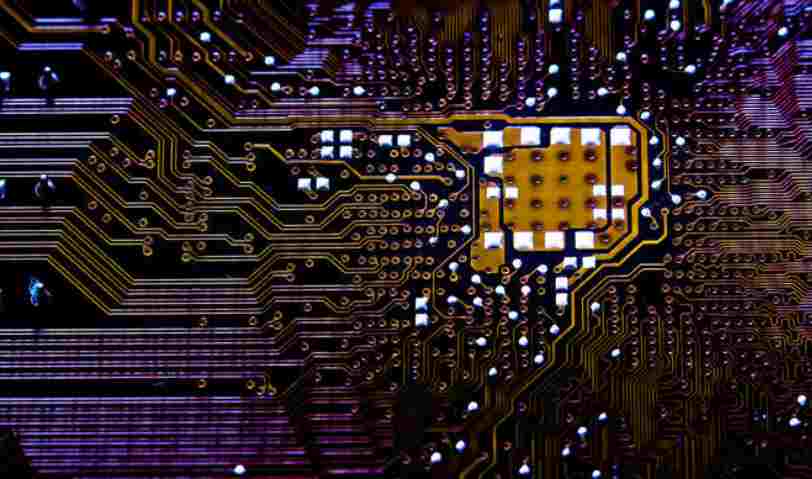


Just upload Gerber files, BOM files and design files, and the KINGFORD team will provide a complete quotation within 24h.