
Professional PCB manufacturing and assembly
Building 6, Zone 3, Yuekang Road,Bao'an District, Shenzhen, China
+86-13410863085Mon.-Sat.08:00-20:00

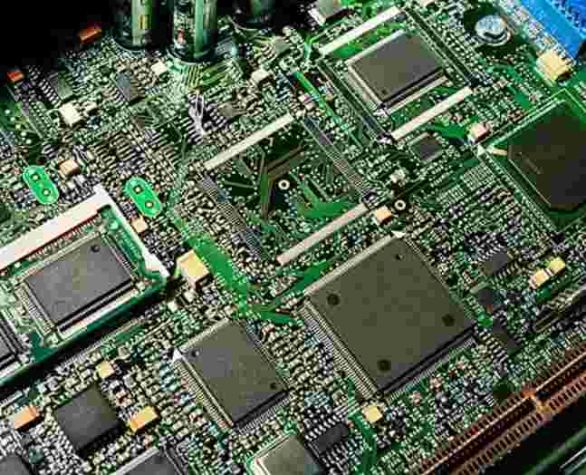
PCB is printed circuit board, short for printed board, is one of the important components of the electronics industry. Almost every electronic device, from electronic watches and calculators to large computers, communication electronics and military weapon systems, where there are electronic components such as integrated circuits, uses printed boards in order to make the electrical interconnection between the components. The printed circuit board is composed of an insulating base plate, connecting wires and a welding pad for assembling welded electronic components. It has the dual functions of conductive circuit and insulating base plate. It can replace the complex wiring, realize the electrical connection between the components in the circuit, not only simplifies the assembly of electronic products, welding work, reduce the traditional way of wiring workload, greatly reduce the labor intensity of workers; And reduce the volume of the machine, reduce the cost of products, improve the quality and reliability of electronic equipment.

Printed circuit board has good product consistency, it can adopt standardized design, conducive to the realization of mechanization and automation in the production process. At the same time, the whole printed circuit board can be used as an independent spare part, which is convenient for the exchange and maintenance of the whole machine products. At present, PCB circuit board has been widely used in the production of electronic products.
Printed circuit board Z early use is paper - based copper-coated printed board. Demand for printed boards has risen dramatically since the advent of semiconductor transistors in the 1950s. Especially with the rapid development and wide application of integrated circuit, the volume of electronic equipment is getting smaller and smaller, and the density and difficulty of circuit wiring are getting bigger and bigger, which requires the printed board to be updated constantly. At present, the variety of printed board has developed from pcb single panel to pcb double panel, pcb multilayer board and flexible board; The structure and quality have been developed to the degree of ultra-high density, miniaturization and high reliability. New design methods, design supplies and board - making materials, board - making technology continue to emerge. In recent years, a variety of computer aided design printed circuit board applications have been popularized and promoted in the industry, in specialized printed board manufacturers, mechanized, automated production has completely replaced manual operation.

Do you know why PCB manufacturers manufacture PCB and what functions they have in electronic equipment? Follow the small edition of the circuit board manufacturer to learn it!
(1)PCB provides mechanical support for fixing and assembling various electronic components such as integrated circuits, realizes wiring and electrical connection or electrical insulation between various electronic components such as integrated circuits, and provides required electrical characteristics.
(2)PCB provides solder resistance graphics for automatic welding and identification characters and graphics for component insertion, inspection and maintenance.
(3) Electronic equipment using PCB printed board, because of the consistency of similar printed board, avoid manual wiring errors, and can realize the automatic insertion or installation of electronic components, automatic soldering, automatic detection, ensure the quality of electronic products, improve labor productivity, reduce costs, and easy maintenance.
(4) Provide the electrical characteristics, characteristic impedance and EMC characteristics required for the circuit in high speed or high frequency circuits.
(5) Printed boards embedded with passive components provide certain electrical functions, simplify electronic installation procedures, and improve product reliability.
(6) It provides an effective chip carrier for miniaturized chip packaging of electronic components in large-scale and super-large-scale electronic packaging components.
The increased density of integrated circuit packages has led to a high concentration of interconnects, which makes the use of multi-substrate necessary. In the layout of printed circuits, unforeseen design problems arise, such as noise, stray capacitance, crosstalk, etc. Therefore, PCB design must be committed to make the signal line length Z small and avoid parallel routes. Obviously, these requirements cannot be satisfactorily answered in a single panel, or even in a dual panel, due to the limited amount of intersections that can be achieved. In the case of a large number of interconnect and cross demand, the board must be expanded to more than two layers to achieve a satisfactory performance, so the emergence of multilayer pcb. Therefore, the original intention of manufacturing multilayer PCBS is to provide more freedom in selecting suitable routing paths for complex and/or noise-sensitive electronic circuits. Multilayer PCBS have at least three conductive layers, two of which are on the outer surface, while the remaining layer is synthesized within the insulating board. The electrical connection between them is usually achieved by plated through holes in the cross-section of the circuit board. Unless otherwise noted, multilayer printed circuit boards, like dual panels, are generally plated through - hole plates.

Multi substrate is made by stacking two or more layers of circuits on top of each other with reliable p recon figured interconnections. Since drilling and plating are done before all the layers are rolled together, this technique violates the traditional fabrication process from the start, which are made up of traditional double panels, the outer layer is made up of separate single panels. Before rolling, the inner substrate will be drilled, electroplated through holes, patterned transfer, developed, and etched. The outer layer to be drilled is the signal layer, which is plated in such a way as to form a ring of balanced copper at the inner edge of the through hole. The layers are then rolled together to form a multi-substrate that can be connected by wave soldering.
Crushing may be done in a hydraulic press or in an over pressure chamber (autoclave). In a hydraulic press, the prepared material (for pressure stacking) is placed under cold or preheated pressure (materials with high glass transition temperature are placed in a temperature of 170-180 ℃). The glass transition temperature is the temperature at which the amorphous region of an amorphous polymer (resin) or part of a crystalline polymer changes from a hard, rather brittle state to a viscous, rubbery state.
Multi substrate is used in specialized electronic equipment (computers, military equipment), especially in the case of weight and volume overload. However, this can only be achieved by the increased cost of multiple substrates in exchange for the increased space and reduced weight. Multi substrate is also very useful in high-speed circuits. They can provide PCB designers with more than two layers of surface to lay wires on, and provide large ground and power areas.
What do you need to do before pcb proofing?
Jan 14,2023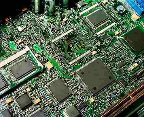


Just upload Gerber files, BOM files and design files, and the KINGFORD team will provide a complete quotation within 24h.