
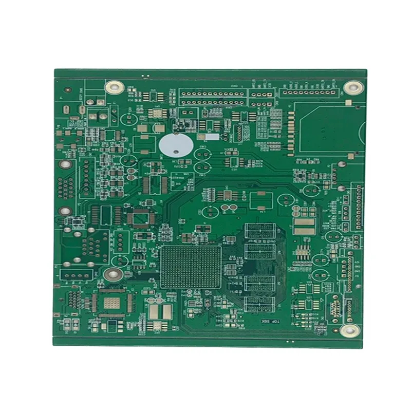
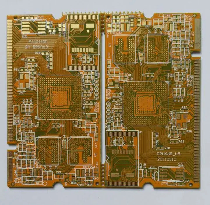
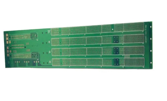
Professional PCB manufacturing and assembly
Building 6, Zone 3, Yuekang Road,Bao'an District, Shenzhen, China
+86-13410863085Mon.-Sat.08:00-20:00

Development History of PCB Assembly Technology and PCB Wire Mesh Knowledge
PCB manufacturing, PCB design and PCBA processing manufacturers explain the history of PCB assembly technology and PCB stencil knowledge
From 1903 to now, from the perspective of application and development of PCB assembly technology, it can be divided into three stages.
1. PCB in through hole insertion technology (THT) stage
Role of metallized hole:
(1) Electrical interconnection - signal transmission
(2) Support components --- reduction of pin size limit through-hole size
a. Pin rigidity
B. Requirements for automatic insertion
Ways to increase density:
(1) Reduce the size of device hole, but limited by the rigidity of component pin and the insertion accuracy, the hole diameter is ≥ 0.8mm
(2) Reduced line width/spacing: 0.3mm-0.2mm-0.15mm-0.1mm
(3) Increase the number of layers: single side - double side - 4 layers - 6 layers - 8 layers - 10 layers - 12 layers - 64 layers
2. Surface Mount Technology (SMT) PCB
Function of through hole:
It only plays the role of electrical interconnection. The hole diameter can be as small as possible, or it can be plugged.
Main ways to increase density:
① The size of via decreases sharply: 0.8mm-0.5mm-0.4mm-0.3mm - 0.25mm
② The structure of vias has changed substantially:
a. Advantages of buried blind hole structure: increase wiring density by more than 1/3, reduce PCB size or layers, improve reliability, improve characteristic impedance control, and reduce crosstalk, noise or distortion (due to short lines, small holes)

b. Hole in pad eliminates relay holes and connections
③ Thinning: double-sided plate: 1.6mm - 1.0mm - 0.8mm - 0.5mm
④ PCB flatness:
a. Concept: warpage of PCB board and coplanarity of connecting plate surface on PCB board.
b. PCB warpage is a comprehensive result of residual stress caused by heat and machinery
C. Surface coating of connecting disc: HASL, electroless plating NI/AU, electroplating NI/AU
3. Chip level package (CSP) stage PCB
CSP has begun to enter a rapid change in its development, promoting the continuous development of PCB technology, and PCB industry will move towards the laser era and nano era.
PCB stencil knowledge
PCB steel mesh
Stencils, also known as SMT Stencil: it is a special SMT mold; Its main function is to help the deposition of solder paste; The purpose is to transfer the exact amount of solder paste to the exact position on the empty PCB.
With the development of SMT process, SMT steel mesh (SMT template) is also used in adhesive process. SMT steel mesh is used to print the solder paste in the semi liquid and semi solid state onto the pcb board. Most of the current popular circuit boards use surface mount (SMT) technology except the power board. There are many surface mount pads on the pcb board, that is, no through hole welding. The holes on the steel mesh are exactly corresponding to the pads on the PCB board. When manually brushing tin, use a horizontal hard brush to brush the solder paste in the semi liquid and semi solid state onto the PCB board through the holes on the steel mesh, Then the components are pasted up through the mounter, and then formed by reflow welding.
Steel mesh was originally made of wire mesh, so it was called mask at that time. At first, it was nylon (polyester) mesh. Later, due to the durability, there were iron wire mesh, copper wire mesh, and finally stainless steel wire mesh. However, no matter what kind of screen is made of, it has the disadvantages of poor molding and low precision.
With the development of SMT and the higher requirements for mesh, steel mesh will be produced. Affected by the material cost and the manufacturing process, the original steel mesh was made of iron/copper plate, but also because it was easy to rust, stainless steel mesh replaced them, which is now the steel mesh (SMT Stencil).
Fabrication method of smt steel mesh
There are three methods for making steel mesh:
Chemical etching:
Apply a layer of acid proof adhesive on the steel plate to remove the adhesive at the place where the opening is required, expose the steel plate, and etch the steel plate with acid to form the opening. This kind of steel plate is the cheapest several hundred pieces, of course, the use effect is the worst.
Electroforming:
The inner wall and chamfer of the opening are electroformed on the basis of laser engraving, making the inner wall of the opening very smooth, which is conducive to tin. This steel plate is very expensive. It is not used unless there are special requirements for the manufacturing process.
Laser engraving:
It is very simple to use the laser to directly punch holes at the places where openings are needed. This kind of steel plate is generally about 800 pieces, which is the most used.
At present, more than 95% of steel meshes in SMT industry are made by laser cutting.
Steel mesh opening requirements
Opening requirements for various types of components
The outer three layers of CHIP type components are increased by 10~15 [%] according to the area, keeping the inner distance unchanged,
Then modify according to the lead requirements
The length of IC components (including row plug) is increased by 0.1-0.20mm outward, and the width is required to be modified if lead is installed, which can be widened appropriately
Resistance and capacitance removal elements, with a length of 0.1mm added outwards. Width can be modified according to lead requirements
Other components are the same as the above requirements.
Acceptance of smt steel mesh
Steel mesh tension 35 ≤ F ≤ 50 (N/cm) Tension error: F ≤ 8 (N/cm)
Appearance of steel mesh: no scratches or bumps on the mesh surface
Before the production of the new stencil, the stencil shall be correctly installed on the printing machine, and 2~5 plates shall be trial printed to confirm the printing effect. After the trial production is passed, the production time shall be recorded in the relevant documents of stencil management.
Printing format requirements for smt stencil
When one board and one net are used, the opening figure shall be centered
When two different PCB boards are opened on the same steel mesh, the edge spacing between the two boards is required to be 30mm
When two same PCBs are opened on one piece of steel mesh, it is required that the spacing between two 180 ° plates is 30mm
What kind of PCB should be engraved with laser steel mesh
Generally, it is only the chip circuit that needs to be engraved with a steel mesh. The steel mesh is mainly used for printing solder paste. Solder paste is paste. Solder paste is missed on the bonding pad, and then the chip components are put on and put into the furnace. The devices are welded after melting with high-temperature solder paste.


Just upload Gerber files, BOM files and design files, and the KINGFORD team will provide a complete quotation within 24h.