
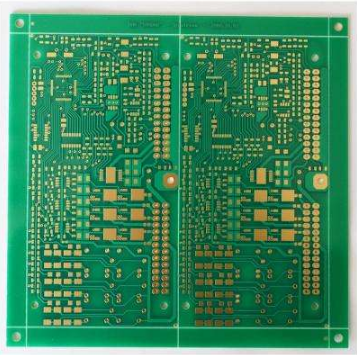
Professional PCB manufacturing and assembly
Building 6, Zone 3, Yuekang Road,Bao'an District, Shenzhen, China
+86-13410863085Mon.-Sat.08:00-20:00

There are several reasons for laying copper on PCB:
1. EMC can shield large areas of ground or power supply copper, and some special areas, such as PGND, play a protective role.
2. PCB copy process requirements. In general, to ensure the electroplating effect or the lamination does not deform, copper is laid on PCB layers with less wiring.
3. Signal integrity requirements: provide a complete return path for high-frequency digital signals, and reduce the wiring of DC network. Of course, there are also reasons such as heat dissipation, copper coating required for installation of special devices, etc.
The Function and Significance of Laying Copper on PCB
1. The function of laying copper on PCB is to reduce the ground wire impedance (a large part of the so-called anti-interference is caused by the reduction of ground wire impedance). There are a lot of spike pulse currents in digital circuits, so it is more necessary to reduce the ground wire impedance. It is generally believed that the circuit composed of digital devices should be paved with a large area of ground, while for analog circuits, the ground wire loop formed by copper coating will cause electromagnetic coupling interference more than it costs (except for high-frequency circuits). Therefore, not all circuits need to be paved with copper (BTW: the laying performance of mesh copper is better than that of the whole block)
2. The significance of copper laying in the circuit lies in: 1. The copper laying is connected with the ground wire, which can reduce the loop area; 2. Large area copper laying is equivalent to reducing the resistance of ground wire and voltage drop. In terms of these two points, both digital ground and analog ground should be paved with copper to increase the anti-interference capability. In addition, in high frequency, digital ground and analog ground should be paved with copper separately, and then connected with a single point. The single point can be wound several times on a magnetic ring with a wire, and then connected. However, if the frequency is not too high, or the working conditions of the instrument are not bad, it can be relatively relaxed. The crystal oscillator can be regarded as a high-frequency emission source in the circuit. You can lay copper around it, and then ground the shell of the crystal oscillator, which will be better.
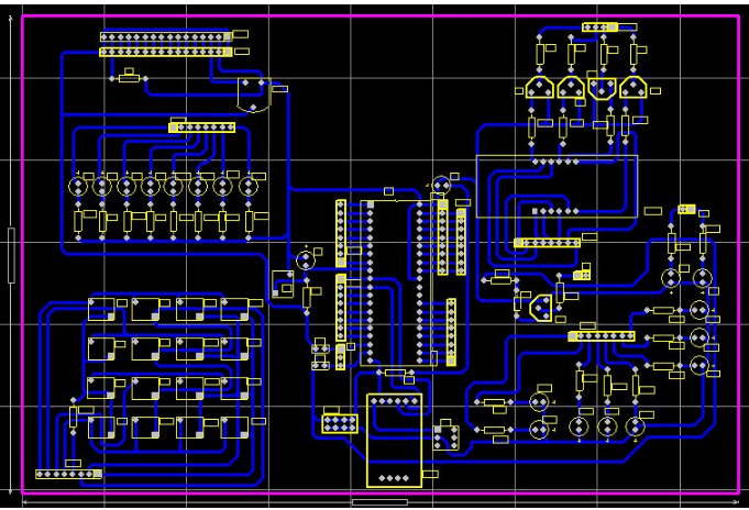
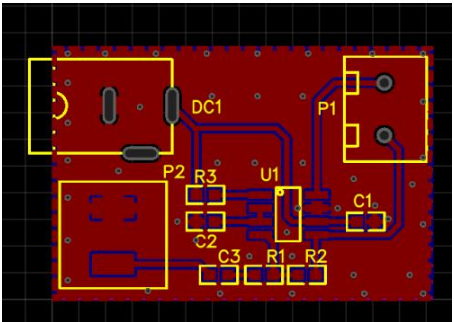
The most basic knowledge of PCB board reading
PCB copy is to scan the finished boards made by others, and then use the copy software to simulate PCB wiring, size, etc. to make PCB files, and then make boards according to PCB files. The name of copy means to copy the design of others. PCB design is to design circuit schematics according to your own ideas and realize the functions required by circuit designers. The difference between them is that PCB design is forward research and development, while PCB copy is reverse research and development.
Question 2: How to manually copy PCB?
First, you need to know the components on your PCB before you can copy them. After you know the components, you can draw a sketch of the circuit with a pen facing the PCB, and then you can draw it in the software. In addition, some parts that cannot be seen under the components need to be removed and then welded on. Those that can be measured with a multimeter need not be removed.
Question 3: How to copy high-precision PCB?
The accuracy of board copying depends on two aspects, one is the accuracy of the software, the other is the accuracy of the original image. For the accuracy of the software, there is no precision limit when using 32-bit floating point representation, so the most important thing is the accuracy of the original scanned image. For example, if you take a picture with 1 million pixels, you can wash a 5-inch picture, but if you want to wash it into a 20 inch picture, you can't see it clearly, The truth is the same, so for a circuit board with high accuracy requirements, if you want to copy a PCB with high accuracy, you should choose a higher DPI when scanning.
DPI means the number of points per inch. That is to say, the distance between every two points on the scanned image is 1000/DPI, in mils
If the DPI is 400, the distance between two points on the image is 1000/400=2.5 mil, that is, the accuracy is 2.5 mil
This is the most scientific basis, so some people say that the accuracy can be less than 1mil, which is a prerequisite. In fact, the board reading accuracy mainly depends on the original scanning accuracy.
To sum up, when scanning a board, the DPI should be set according to the accuracy required by the actual board. If the accuracy requirements such as the cell phone board sub line spacing are less than 1mil, then the DPI should be set above 1000DPI. At present, scanners on the market can meet this condition.
The higher the DPI is, the clearer the picture is and the higher the accuracy is. However, the disadvantage is that the picture is too large and requires high hardware, so it should be set according to the specific situation. For boards with general accuracy, it is good to use 400DPI. For mobile phone boards, it can be set above 1000DPI.
Question 4: How to select board copying software?
The quality of the board reading software mainly depends on whether the functions are complete. It is better to do all the work in the board reading software, so that the efficiency is high. It is best to support PROTEL99SE in the placement of components. At present, 99SE has a very rich component library, which can be downloaded from the Internet. This is also a very important thing. The era of making components by hand has passed, because there are hundreds of elements in many BGP component packages. It is too expensive to build components by hand.
In order to ensure the stability and reliability of the circuit, a large piece of copper sheet shall be connected to the power supply or ground in PCB design, which can reduce the noise and interference of the circuit. Therefore, the problem of copper laying on the network is involved. For complex circuit boards, there are many connections and many isolations on the copper laying. If this problem is not solved properly, copper laying cannot be realized. Therefore, we must define a network to lay copper ("the same network is connected, but different networks are isolated"). Simply filling all PCNs with copper skin will lead to end circuits. This is also a key issue to measure PCB copy software.


Just upload Gerber files, BOM files and design files, and the KINGFORD team will provide a complete quotation within 24h.