
Professional PCB manufacturing and assembly
Building 6, Zone 3, Yuekang Road,Bao'an District, Shenzhen, China
+86-13410863085Mon.-Sat.08:00-20:00

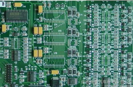
PCB copy refers to the process of PCB copy of existing electronic products or physical circuit boards. Different from PCB design, PCB copy is a reverse research method. Through a series of reverse technology research such as professional PCB reverse schematic software, a full set of production materials such as product PCB files, BOM lists, SCH schematic files are derived, and then used in the process of product cloning.
In many years of PCB copying practice, Godson Century has accumulated rich experience, mastered hundreds of reverse deduction methods, and combined with the latest PCB reverse schematic software, it can provide customers with various high-frequency board reverse drawing schematics and modifications, reverse design and reverse drawing schematics of multi-layer blind hole boards, reverse design of 8-layer server computer motherboard schematics, reverse drawing schematics of more than 10 layer PCB files, and so on. Then the problem arises. What should be paid attention to in the process of reversing the schematic diagram? Dragon Core Century has summarized the following experience:
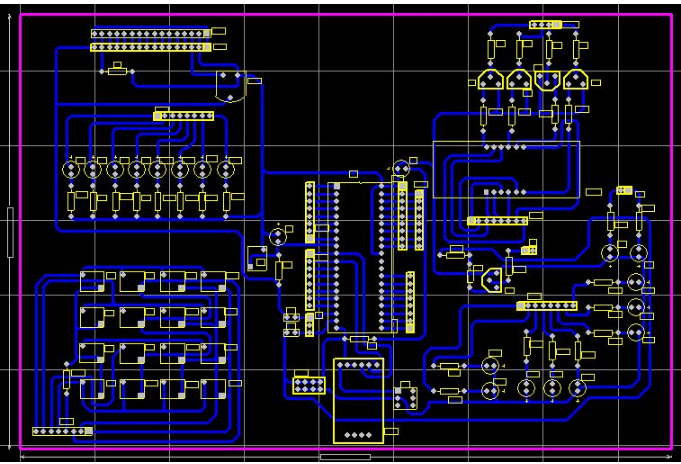
First, reasonably divide the functional areas
When reverse designing the schematic diagram of a good PCB, reasonable division of functional areas can help engineers reduce some unnecessary trouble and improve the efficiency of drawing. In general, components with the same function on a PCB board will be arranged in a centralized manner, so that functional division can provide convenient and accurate basis for reversing schematic diagrams. However, the division of this functional area is not arbitrary. It requires engineers to have a certain understanding of electronic circuit related knowledge. First, find out the core components of a functional unit, and then find out other components of the same functional unit according to the routing connection to form a functional partition. The formation of functional partition is the basis of schematic drawing. In addition, the number of components on the circuit board is skillfully used in the process of functional zoning, which is conducive to faster functional zoning.
II. Alignment of reference piece
The reference parts can be said to be the main parts to be used at the beginning of schematic drawing. After the reference parts are determined, the drawing can be carried out according to the pins of these reference parts to ensure the accuracy of schematic drawing to the greatest extent. For engineers, the determination of reference pieces is not very complicated. Generally, components that play a major role in the circuit can be selected as reference pieces. They are generally large in size and have many pins, which are convenient for drawing. For example, integrated circuits, transformers, crystal tubes, etc. can all be used as appropriate reference pieces.
Third, correctly distinguish the lines and reasonably draw the wiring
For the distinction of ground wire, power wire and signal wire, engineers also need to have relevant knowledge of power supply, circuit connection, PCB wiring, etc. The distinction of these circuits can be analyzed from the connection of components, the width of circuit copper foil and the characteristics of electronic products. In wiring drawing, in order to avoid line crossing and interpenetration, a large number of grounding symbols can be used for ground wires, different lines of different colors can be used for various lines to ensure clear identification, special marks can also be used for various components, and even unit circuits can be drawn separately and combined at last.
Fourth, master the basic framework and learn from similar schematic diagrams
Engineers need to be proficient in the frame composition and schematic drawing of basic electronic circuits. They should not only be able to directly draw the basic composition forms of some simple and classic unit circuits, but also be able to form the overall frame of electronic circuits. In addition, PCB products of the same type have certain similarities in schematic diagrams, so engineers can fully learn from similar circuit diagrams to reverse the schematic diagrams of new products based on the accumulation of experience.
Fifth, check and optimize
After the schematic diagram is drawn, the reverse design of PCB schematic diagram can be said to be completed only after the test and verification. The nominal values of components sensitive to PCB distribution parameters need to be checked and optimized. According to the PCB file diagram, the schematic diagram needs to be compared, analyzed and checked to ensure that it is completely consistent with the file diagram. If the schematic layout is found to be inconsistent with the requirements during the check, the schematic will be adjusted until it is completely reasonable, standard, accurate and clear.


Just upload Gerber files, BOM files and design files, and the KINGFORD team will provide a complete quotation within 24h.