
Professional PCB manufacturing and assembly
Building 6, Zone 3, Yuekang Road,Bao'an District, Shenzhen, China
+86-13410863085Mon.-Sat.08:00-20:00

1、 Open the pcb copy board design drawing on the computer, light up the short circuit network, and see where it is the nearest and easiest to connect to one. Pay special attention to the short circuit inside the IC.
2、 If manual welding is used, good habits should be formed:
1. Before welding, visually check the PCB copy, and use a multimeter to check whether the key circuits (especially the power supply and ground) are short circuited;
2. Every time a chip is welded, use a multimeter to test whether the power supply and ground are short circuited;
3. Do not throw the soldering iron randomly during welding. If you throw the soldering tin onto the solder leg of the chip (especially the surface mount components), it will not be easy to find.
3、 A short circuit was found. Take a board to cut lines (especially for single/double layer boards). After cutting lines, power on each function block separately and gradually eliminate it.
4、 Short circuit positioning and analysis instruments are used, such as PROTEQ CB2000 short circuit tracker in Singapore, QToard circuit short circuit detector in the UK (most of the equipment of Longxin Century, a professional b50 short circuit tracker in Hong Kong Lingzhi Technology, POLAR ToneOhm950 multi-layer board copying company, are foreign advanced equipment)
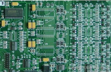
5、 If there is a BGA chip, because all the solder joints are covered by the chip and cannot be seen, and it is also a multilayer board (more than 4 layers), it is better to separate the power supply of each chip during the design, and connect it with a magnetic bead or a 0 ohm resistance. In this way, when the power supply is short circuited to the ground, disconnect the magnetic bead detection, and it is easy to locate a chip. Because BGA is difficult to weld, if it is not automatically welded by the machine, it will short circuit the adjacent power supply and the two welding balls.
6、 Be careful when welding small surface mount capacitors, especially power filter capacitors (103 or 104), which are large in number, can easily cause short circuit between power supply and ground. Of course, sometimes the capacitor is short circuited due to bad luck, so the best way is to check the capacitor before welding.
We all understand the principle of taking precautions. Dragon Core Century, a professional pcb board copying company, said that we must develop a good habit of inspection in the design of pcb board copying. Adherence to the above six habits will be more convenient in practical operation.
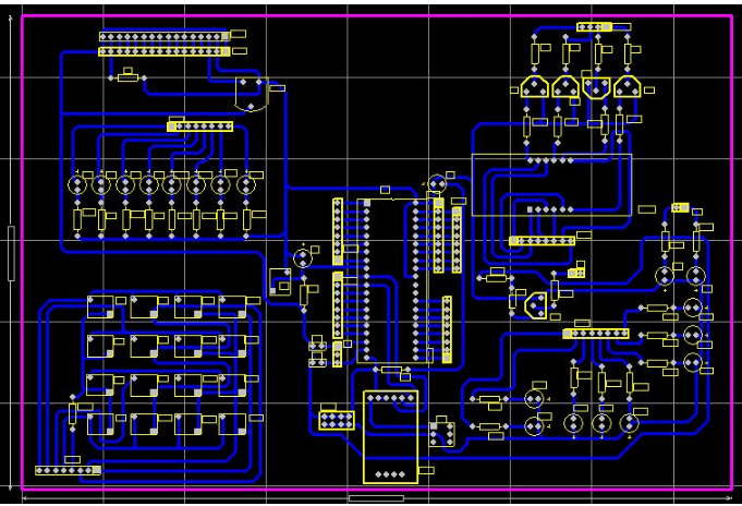
Reading method of double-layer circuit board:
1. Two BMP pictures are saved on the upper and lower layers of the scanning line double-layer circuit board.
2. Open the board copying software Quickpcb2005, click "File" and "Open base map" to open a scan image. Enlarge the screen with PAGEUP, see the PCB pad, press PP to place a pad, see the line and press PT to route... Just like a child tracing, draw once in this software, and click "Save" to generate a B2P file.
3. Click "File" and "Open base map" again to open another layer of scanned color map;
4. Click "File" and "Open" again to open the previously saved B2P file. We can see that the board just copied is stacked on this picture - the same PCB board, the holes are in the same position, but the circuit connections are different. So we press "Options" - "Layer Settings", and turn off the display of lines and silk screen on the top layer here, leaving only multi-layer vias.
5. The vias on the top layer are in the same position as those on the bottom layer picture. Now we can trace the lines on the bottom layer as we did in childhood. Click "Save" again - the B2P file now has two layers of data: the top layer and the bottom layer.
6. Click "File" and "Export as PCB File" to get a PCB file with two layers of data. You can change the board again or issue the schematic diagram again or directly send it to the PCB plate making factory for production
Reading method of multilayer circuit board:
In fact, copying four layers of boards means repeatedly copying two double-sided boards, and copying six layers of boards means repeatedly copying three double-sided boards... The reason why copying multilayer circuit boards is so daunting is that we cannot see the wiring inside them. How can we see the inner world of a precision multilayer board—— layered.
There are many layering methods, such as liquid medicine corrosion and tool stripping, but it is easy to divide the layers too much and lose data. Experience tells us that sandpaper grinding is the most accurate.
When we finish copying the top and bottom layers of multilayer circuit boards, we usually use sandpaper to polish the surface layer to show the inner layer; Sandpaper is a kind of ordinary sandpaper sold in hardware stores. Generally, the PCB is tiled, then the sandpaper is pressed and evenly rubbed on the PCB (if the board is very small, the sandpaper can also be tiled, and the PCB is pressed and rubbed on the sandpaper with a finger). The key point is to pave it so that it can be ground evenly.
The silk screen and green oil are usually wiped off, and the PCB copper wire and copper skin should be wiped well for several times. Generally speaking, the Bluetooth board can be wiped in a few minutes, and the memory module takes about ten minutes; Of course, with great strength, it will take less time; It will take a little more time.


Just upload Gerber files, BOM files and design files, and the KINGFORD team will provide a complete quotation within 24h.