
Professional PCB manufacturing and assembly
Building 6, Zone 3, Yuekang Road,Bao'an District, Shenzhen, China
+86-13410863085Mon.-Sat.08:00-20:00

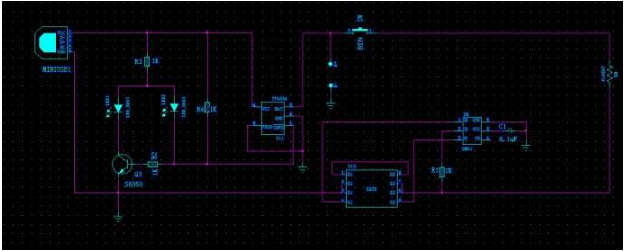
To put it simply, the technical realization process of PCB copying is to scan the circuit board to be copied first, and record the models, parameters and positions of all components, especially the directions of diodes, triodes and IC notches. Then dismantle the components to make a bill of materials (BOM) and arrange material procurement. The blank board is scanned into a picture and restored to a PCB drawing file after being processed by the board copying software. Then send the PCB file to the plate making factory for board making. After the board is made, the purchased components are welded to the made PCB board. In this way, a board like the original board is born. Of course, this is not the end of the work. The last and most important step is to test and debug the circuit board. Only when the test results prove that the electronic technical performance of the copied board is the same as that of the original board, can the work be completed.
When the boards are relatively large and the components are relatively large, there are often some difficulties in debugging, but if you master a set of reasonable debugging methods, you will get twice the result with half the effort. First, roughly observe whether there are problems on the board, such as obvious cracks, short circuits, open circuits, etc. If necessary, check whether the resistance between the power supply and the ground wire is large enough.
Then there is the installation of components. If you are not sure to ensure the normal operation of independent modules, you'd better not install them all, but part by part (for small circuits, you can install them all at once), so that it is easy to determine the fault range and avoid having no way to start when encountering problems.
Generally speaking, the power supply part can be installed first, and then power on to detect whether the power supply output voltage is normal. If you are not sure when powering on (even if you are sure, it is recommended to add a fuse in case), you can consider using an adjustable regulated power supply with current limiting function. Preset the overcurrent protection current, then slowly increase the voltage of the stabilized voltage power supply, and monitor the input current, input voltage and output voltage. If there are no over-current protection problems during the upward adjustment and the output voltage is normal, the power supply is OK. Otherwise, disconnect the power supply, find the fault point, and repeat the above steps until the power supply is normal.
Next, gradually install other modules. After each module is installed, power on and test it. Follow the above steps when powering on to avoid burning components due to overcurrent caused by design errors or/and installation errors.
PCB copying has many names in the industry, such as circuit board copying, circuit board cloning, circuit board copying, PCB cloning, PCB reverse design or PCB reverse research and development. That is to say, on the premise that there are real electronic products and real circuit boards, reverse analysis of circuit boards is carried out by means of reverse research and development technology, and 1:1 restoration of PCB documents, bill of materials (BOM) documents, schematic diagram documents and other technical documents of the original products as well as PCB silk printing production documents is carried out. Then, these technical documents and production documents are used for PCB manufacturing, component welding, flying pin testing, and circuit board debugging, Complete the complete copy of the original circuit board template.
How to do a good job of pcb board reading scheme of three-layer core routing switch board
The three-layer core route switch board is a very typical high-speed board. Morning Core Technology, a pcb board reading company, has formulated detailed solutions according to the difficulties of the board. The following are the specific technical solutions for pcb board reading:
First of all, the difficulty of this switch board is that it has strict timing requirements. The BCM56601 chip scheme is adopted, with RLDRAM, DDRII SDRAM, TCAM, multiple pairs of 3.125G high-speed signals on the board, 48 pairs of 1.25G signals, and each pair is 13 inches long; Secondly, the impedance control is also quite strict. There are many kinds of power supplies. There are 8 kinds of currents above 6 A, and a large number of phase-locked loops; More than 25000 board PINs, a large number of network rules
According to the above difficulties, Chenxin pcb board company's solution is to analyze the data in detail to calculate the timing, and HSPICE simulates the PCB wiring rules of 1.25G signal and 3.125G signal. The routing topology of RLDRAM, DDRII SDRAM and TCAM is determined by pre simulation, and their timing is confirmed by post simulation. Through the current calculation software, the current wiring channel is designed reasonably on PCB. Multi person concurrent design ensures board progress.


Just upload Gerber files, BOM files and design files, and the KINGFORD team will provide a complete quotation within 24h.