
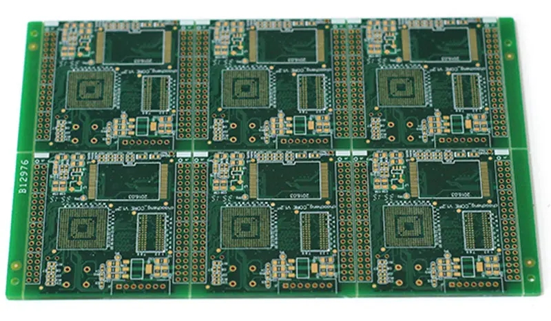
Professional PCB manufacturing and assembly
Building 6, Zone 3, Yuekang Road,Bao'an District, Shenzhen, China
+86-13410863085Mon.-Sat.08:00-20:00

PCB Factory: Technical Trend of Embedded Electronic Component Substrate
Foreword Nowadays electronic components or PWBs have changed a lot. 1C packaging is developing from the miniaturization of chip size to the three-dimensional installation of memory, etc. Passive components are accelerated from chip components to ceramic clad components, and are developing towards embedded passive component substrate module or package with 1C. They begin to move towards resin based substrates, especially towards embedding passive and active component substrates. Silicon (Si) chips also have integrated passive component chips, which are the insert substrates suitable for 1C packaging, accelerating the development of embedded passive component substrates. This paper describes the technical trend of embedded electronic component substrate.
Online supply chain solutions for electronic industry, such as component purchase, PCB customization and material selection, are provided to meet the comprehensive needs of small and medium-sized customers in the electronic industry in a one-stop manner.
The trend of electronic component technology With the miniaturization, high performance and multi-function of electronic devices, IC packaging has developed from QFP and TCP of a single chip to small BGA and CSP, to wafer level CSP (d) with the same size as the bare chip. In addition, the development of packaging (MCP, Multi ChipPackage) or modularization (MCM, Multi ChipModule) for two-dimensional element or three-dimensional installation of heterogeneous IC chips is also accelerating, and the development of IC chip based system LSI is also very active. Then, due to the complexity of system LSI design, he has been engaged in PCB technology for a long time and has published many articles in the journal.
However, due to the brittleness of ceramic substrate, it is not suitable for large thin substrate, which is limited to special small modules or packages. In addition, when the substrate heats up, dozens of percent sintering shrinkage occurs, which makes it impossible to conduct electrical inspection and embed high-precision components. It is difficult to form a resistance with an error value of ± 1% due to the inability to trim before and after sintering. Therefore, the fluctuation degree of sintering shrinkage is.
Trend of Si Substrate for Integrated Passive Components Up to now, ceramic based substrates occupy the majority of passive component integration and embedded substrate. Recently, however, the integrated passive device (IPD) of LRC passive components formed on Si substrate by semiconductor technology has been introduced. Up to now, although there is no Si chip integrated with passive components, the Si chip can integrate large value passive components that are difficult to be embedded in semiconductor 1C.
The directionality of ceramic chip components Because micro chip devices are difficult to manufacture and install, and the installation efficiency or operability of a single component is very poor, the number of two-dimensional or three-dimensional composite devices with the same or different passive components increases dramatically. Recently, with the rapid increase of mobile phones, the modular trend of carrying 1C is accelerating. However, it is not enough to just stay in the high-performance, multi-function, lightweight and miniaturization of electronic machines. The demand for high-speed, high-frequency and ultra small portable machines with several GHz to tens of GHz bands has increased dramatically. The traditional SMT high-density installation mode, which uses separate manufacturing and combination of substrates and electronic components, is difficult to meet the requirements of improving performance, miniaturization and thinness. Therefore, recently, passive components and 1C have been embedded in the substrate, It can shorten the connection length between components, and also can suppress the LRC delay, noise, heat and other problems caused by wiring. Moving the installation mode from SMT to SMT can not only improve the performance of the electronic machine, realize the lightness and miniaturization of the electronic machine, but also improve the reliability and reduce the overall installation cost due to the reduction of welding positions.
The substrate for embedding passive components in ceramic composite devices can be traced back to the low-temperature sintered glass ceramic substrate developed in the 1970s. lt: The following sintered substrates can be embedded in 800t~900t: sintered thick film resistors or thick film capacitors, which became practical in the mid-1980s (). In this structure, LRC and other devices are printed on the glass ceramic substrate and sintered once after being laminated. However, because the selection range is small, it is generally only used for special purposes. In the second half of the 1980s, barium titanate (BaTiQ Or the technology of printing electrode on the strong electric medium such as ferrite or the strong magnetic body chip, and sintering it into a passive composite element after the lamination ((c)). Due to the lamination and one-time simultaneous sintering of raw chips with different sintering shrinkage or thermal expansion coefficient, technologies highly adaptable to composition or sintering process are required, for which electronic component manufacturers or ceramic manufacturers have made great efforts.
PCB manufacturers, PCB designers and PCBA manufacturers will explain the technical trends of embedded electronic component substrates.

How to calculate the cost of circuit board
Nov 13,2022


Just upload Gerber files, BOM files and design files, and the KINGFORD team will provide a complete quotation within 24h.