How to optimize PCB panel design from the perspective of cost
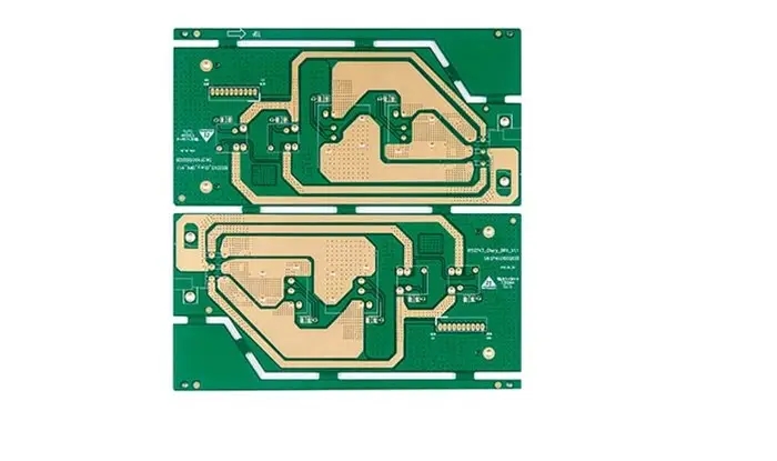
1、 The significance of PCB assembly design After PCB wiring is completed, due to the requirements of PCBA assembly process, it is necessary to perform assembly design for some PCBs with special shapes, so that the subsequent PCBA assembly process can proceed smoothly. In the process of panel assembly design, it is usually necessary to add sidebars and connect one or several PCB units with the sidebars in a certain way to form a PCB shape that meets the PCBA assembly requirements. The panel size will have a direct impact on the material utilization and panel size during PCB production, and even significantly affect the price of PCB. The number, width, position of the edges, the number of PCB units, the arrangement of PCB units, the connection method, and the slot width will all affect the panel size. This paper mainly discusses how to optimize the size of the panel by controlling these influencing factors in the process of panel design, on the premise of meeting the requirements of PCB and PCBA assembly process, so that it can generate high panel utilization and appropriate production panel size when forming PCB production panel, thus obtaining a lower PCB quotation.

2、 Under what circumstances do you need to do the panel design? Under the following circumstances, you need to do the panel processing on PCB to form a panel to meet the PCBA assembly requirements:
(1) The mechanical structure requirements of the PCB design itself (2) The component pads are too close to the PCB board edge, the top layer is less than 4.06 mm, and the bottom layer is less than 5.08 mm (the top layer is less than 0.16 inch, and the bottom layer is less than 0.2 inch) (3) The test points that need soldering are too close to the board edge, the top layer is less than 4.06 mm, and the bottom layer is less than 5.08 mm (the top layer is less than 0.16 inch, and the bottom layer is less than 0.2 inch) (4) The irregular shape or size is too small, The PCBA assembly line cannot be successfully passed. (5) To improve the PCBA assembly production efficiency, the terms and definitions of panel assembly are introduced to explain how to optimize panel assembly from the perspective of cost.


